Semiconductor memory device

Inactive Publication Date: 2006-11-02
CONVERSANT INTPROP MANAGEMENT INC
View PDF9 Cites 12 Cited by
  • Summary
  • Abstract
  • Description
  • Claims
  • Application Information

AI Technical Summary

Benefits of technology

[0028] It is, therefore, an object of the present invention to provide a semiconductor memory device adjusting a bit line over driving period according to a power supply voltage level.

Problems solved by technology

Meanwhile, it is hard to operate the large amount of the BLSAs in a short time by using the core voltage VCORE having a low voltage level.
However, when a level of a power supply voltage is relatively high as shown in FIG. 5C, the over driving operation is performed excessively; and, therefore, the bit line BL is excessively charged.
When the excessive electric charge flows back to the core voltage terminal, a level of the core voltage VCORE becomes unstable.
However, as a result, the circuit substantially wastes a current.
Moreover, when the BLSA is repeatedly driven, the problems abovementioned are further deepened.
As a result, it is very hard to appropriately determine an over driving period in the conventional RTO drive control signal generation block.

Method used


Image

  • Semiconductor memory device
  • Semiconductor memory device
  • Semiconductor memory device

Examples


Embodiment Construction

[0045] Hereinafter, a semiconductor memory device in accordance with the present invention will be described in detail referring to the accompanying drawings.

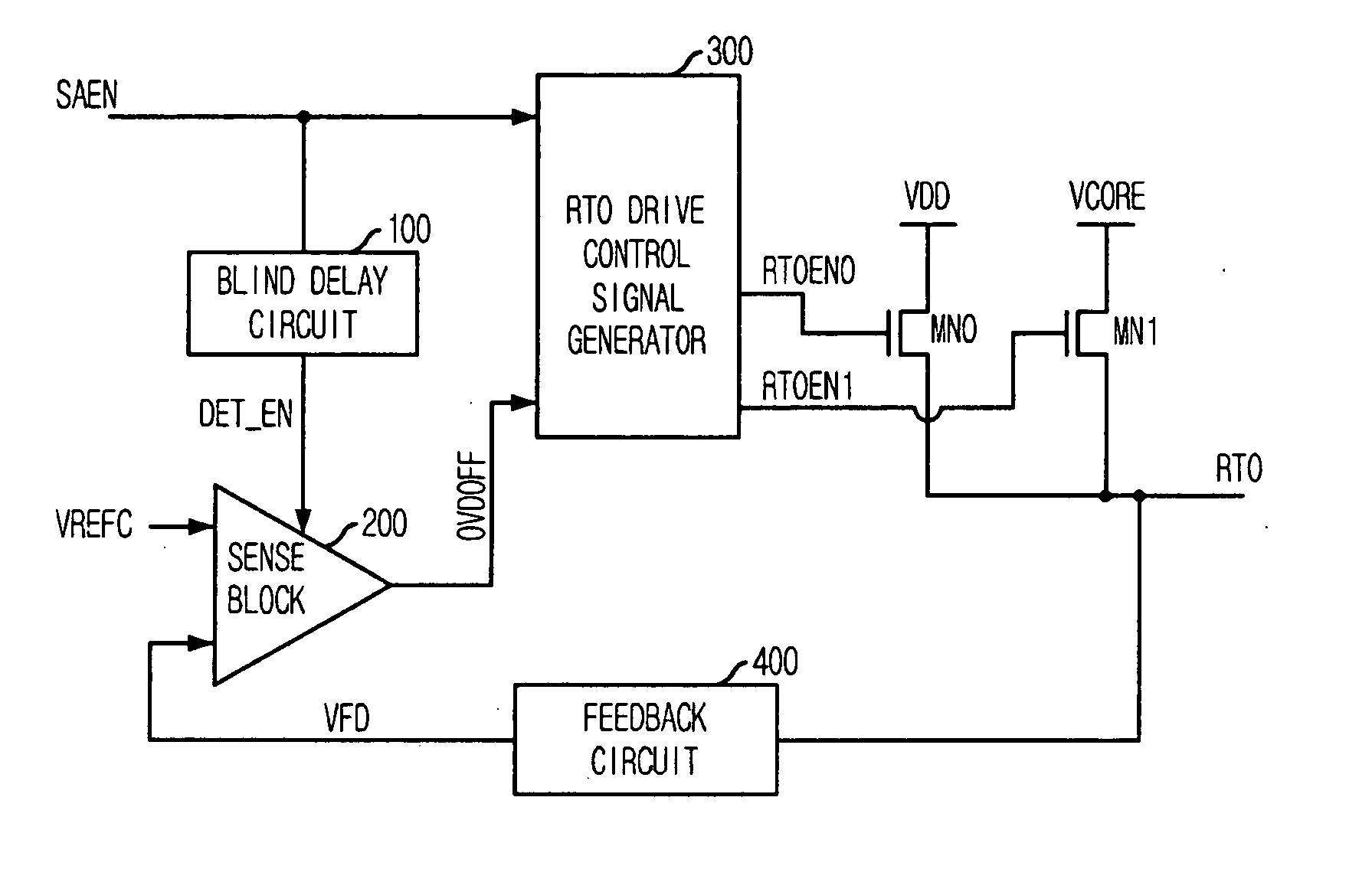
[0046]FIG. 6 is a block diagram describing an RTO drive control signal generation block in accordance with a preferred embodiment of the present invention.

[0047] As shown, the RTO drive control signal generation block includes a blind delay circuit 100, a sense block 200, a RTO drive control signal generator 300, and a feedback circuit 400.

[0048] The blind delay circuit 100 delaying a bit line sense amplifier (hereinafter, referred as BLSA) enable signal SAEN outputs a detection enable signal DET_EN. The sense block 200 compares a reference voltage VREFC with a feedback voltage VFD to output an over driving off signal OVDOFF in response to the detection enable signal DET_EN. The RTO drive control signal generator 300 outputs a first and a second RTO drive control signal RTOEN0 and RTOEN1 in response to the BLSA enable signal...


PUM


Abstract

The present invention provides a semiconductor memory device adjusting a bit line over driving period according to a power supply voltage level. A semiconductor memory device for stabilizing a bit line sense amplifier (hereinafter, referred as BLSA) includes the BLSA operated by a sense amplifier driving voltage; and a controller for comparing a feedbacked sense amplifier driving voltage with a reference voltage to thereby control the sense amplifier driving voltage to the BLSA.

Description

FIELD OF THE INVENTION [0001] The present invention relates to a semiconductor memory device; and, more particularly, to a semiconductor memory device having a bit line over driving scheme and a method for stably supplying a driving voltage to a bit line sense amplifier thereof. DESCRIPTION OF PRIOR ART [0002] As a size of a semiconductor memory is decreased, a level of an internal voltage also becomes lower. Most semiconductor memories include an internal voltage generator generating various kinds of internal voltages for internal operations of the semiconductor memories. Among the various kinds of internal voltages, a semiconductor memory device using a bit line sense amplifier (hereinafter, referred as BLSA) such as a DRAM uses a core voltage for sensing a cell data. [0003] After a word line selected by a row address is activated, data stored in a plurality of memory cell connected to the selected word line are transmitted to each corresponding bit line. Then, each BLSA senses an...

Claims


Application Information

Patent Timeline
IPC IPC(8): G11C7/02
CPCG11C2207/065G11C7/06G11C7/12G11C11/4091G11C11/4094
Inventor DO, CHANG-HO
Owner CONVERSANT INTPROP MANAGEMENT INC
Why Eureka
Try Eureka