Static random access memory architecture

a random access and memory technology, applied in static storage, information storage, digital storage, etc., can solve the problems of increasing the clock frequency of srams, large integrated circuit area, and increasing the clock speed of microprocessors

Inactive Publication Date: 2008-06-19
CISCO TECH INC
View PDF8 Cites 195 Cited by
  • Summary
  • Abstract
  • Description
  • Claims
  • Application Information

AI Technical Summary

Problems solved by technology

Although the memory cells of an SRAM do not need to be continually refreshed, as do those of a dynamic random access memory (DRAM), the number of transistors used for each cell to provide a single memory bit results in a large amount of integrated circuit (IC) area to implement a large SRAM.
In addition to the issues associated with increases in size of SRAMs, microprocessor clock speeds have increased which have increased the clock frequencies of SRAMs.
As recognized by the present inventors, the increasing size and speed issues of SRAMs has made the design of conventional SRAM memories problematic.
In particular, the propagation delay of the voltage differential through the bit line pair becomes large enough so as to prevent reliable detection of the contents of the addressed memory cell in the available time.
In a large SRAM, comprised of many banks, this arrangement quickly consumes IC real estate available for wire tracks.
This implementation is limited, however, by the amount of differential signal that can be driven over the length of wire necessary to couple the banks of memory cells to the sense amplifier.
A drawback of the implementation of FIG. 3 is that once the number of banks has increased beyond a certain point, the length of the bit line pair 93 has increased too much to allow the differential signal to propagate through its length in the time available, preventing the sense amplifier 92 from reading the differential signal reliably.
Further, the necessary number of wire tracks doubles at each level of the SRAM hierarchy, which has obvious scaling difficulties.

Method used


Image

  • Static random access memory architecture
  • Static random access memory architecture
  • Static random access memory architecture

Examples


Embodiment Construction

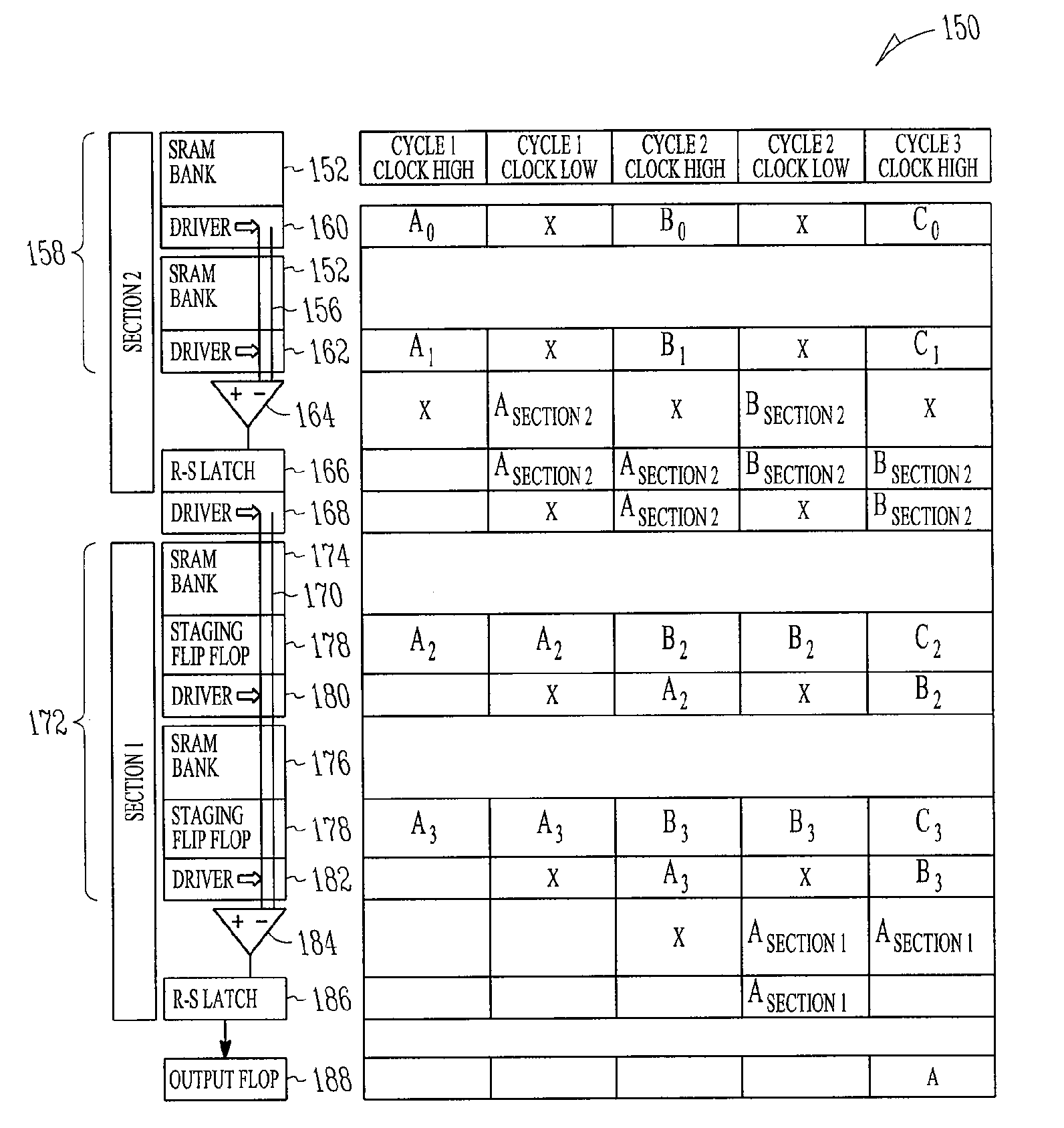
[0036]According to one broad aspect of the invention, disclosed herein is a memory which may be used in a router. In one example, the memory includes a first data bus, a first plurality of banks of SRAM coupled with the first data bus, a first differential sense amplifier receiving the first data bus, and a first output driver receiving the output of the first differential sense amp. The first output driver selectively drives the signal from the first data bus onto a second data bus which has a second plurality of banks of SRAM coupled thereto. A second differential sense amplifier receives the second data bus (as well as the first data bus through the first output driver), and a second output driver selectively drives an output signal which may include data from the first data bus or the second data bus. The memory may be expanded by adding additional data buses coupled with additional SRAM banks. Staging logic or logic gates may be used to temporarily store data from SRAM banks as...


PUM


Abstract

An architecture for a semiconductor static random access memory (SRAM) is described. In one example, a first set or group or stage of SRAM banks are coupled to a first data bus formed using bit line pairs, and a second set or group or stage of SRAM banks are coupled to a second data bus formed using other bit line pairs. The number of banks coupled to each bit line pair is determined by the SRAM's operating frequency and size. Each data bus is coupled to a sense amplifier. The output from the sense amplifier is then coupled to the bit line pair of a group of SRAM banks. This adjacent group has staging logic coupled to each SRAM bank to store the output of the SRAM bank until the contents from the first group is placed on the bit line of the adjacent stage of SRAM banks. The output from either the first stage or from one of the SRAM banks in the adjacent stage's SRAM banks, which had been stored in the adjacent stage's staging logic, is driven to the sense amplifier coupled to the adjacent stage. Successive stages of SRAM banks can be coupled together until an arbitrary number of stages of SRAM banks have been coupled together.

Description

CROSS REFERENCE TO RELATED APPLICATION[0001]This application claims the benefit under 35 U.S.C. 119(e) of U.S. provisional patent application Ser. No. 60 / 416,013 filed Oct. 2, 2002, entitled “STATIC RANDOM ACCESS MEMORY ARCHITECTURE,” the disclosure of which is hereby incorporated by reference in its entirety.TECHNICAL FIELD[0002]This application relates, in general, to semiconductor memories. More specifically, it relates to static random access memory (SRAM).BACKGROUND[0003]An SRAM semiconductor memory is typically comprised of a plurality of memory cells, each memory cell having, for example, four to six transistors. Generally, each memory cell is coupled to a column and row select line which is used to select the individual memory cell, and each memory cell receives its input and drives its output onto a pair of sense lines, typically designated sense and sense complement. For purposes of this description, this pair of sense lines (sense and sense complement) shall be called the...

Claims


Application Information

Patent Timeline
Patent Type & Authority Applications(United States)
IPC IPC(8): G11C11/00G11C8/00
CPCG11C5/063G11C7/065G11C11/413G11C7/1069G11C8/12G11C7/1051
Inventor WONG, BENJAMIN S.
Owner CISCO TECH INC
Why Eureka
Try Eureka