Magnetoresistive memory device

a magnetic memory and memory device technology, applied in semiconductor devices, digital storage, instruments, etc., can solve the problems of circuitry suffering from high threshold voltage (and thus the cell's drain) to potentially go high, and high risk of writing errors

Inactive Publication Date: 2003-09-23
KK TOSHIBA
View PDF5 Cites 173 Cited by
  • Summary
  • Abstract
  • Description
  • Claims
  • Application Information

AI Technical Summary

Problems solved by technology

Electrons are accumulated at the cell's floating gate, causing a bit line associated with a memory cell of higher threshold voltage (and thus the cell's drain) to potentially go high.
The presence of this high drain potential can cause writing errors, especially for those memory cells presently in an erase state (ordinarily, logic data "1" storage state).
Even when word-line closing control is done after completion of each bit data reading, possible stress becomes stronger when compared to the two-value case, resulting in the circuitry suffering from high risks of writing errors.
Although the resistance difference gets larger owing to research and development results in recent years, the application voltage is strictly required to fall within a limited range of from 0.2 to 0.4V; otherwise, the resistance different would decrease thereby making the data judgment more difficult.
Unfortunately, this does not come without accompanying a trade-off: the use of many elements for each cell suffers from reduction of on-chip integration density and per-cell storability; if a 1-transistor / 1-MTJ cell structure is employed for achieving mass-storabilities, then, a reference voltage must be set at a potential level as created by an intermediate resistance that is midway between the resistance values of a spin-antiparallel MTJ element and that of spin-parallel MTJ element, resulting in a read signal amount becoming half-reduced.
Unfortunately as shown in a characteristic diagram of FIG. 29, upon occurrence of excessive potential rise-up beyond a trigger voltage Vpeak entering a negative differential resistance region, read errors can occur causing a read voltage VR to be limited.
Exceeding beyond the trigger voltage Vpeak entering the negative differential resistance region can cause read errors; thus the read voltage VR is limited.
Although D1 with teachings of T-RAM cells fails to suggest sense-amp circuitry per se, execution of the ratio operation would cause similar problems to those in the case of TSD cells.
As far as such architecture is used, even if charge carriers as injected into a gate due to drain avalanche with application of a potentially high drain voltage--"hot" carriers--are less in amount, resultant storage node potential change is significant undesirably.
This precharge voltage reduction causes read errors in some cases.
Further, turning back to the discussion on the read operation, sense MOS transistors of the load and gain cell are designed to perform the ratio operation, although the sense-amp circuitry of FIG. 57 per se does not offer any ratio operability.
The use of such architecture is faced with a problem as to unwanted increase in stresses being applied to the memory cells.
If an attempt is made to lessen such stresses, the resultant memory cells are no longer capable of sufficiently offering the performance required.

Method used


Image

  • Magnetoresistive memory device
  • Magnetoresistive memory device
  • Magnetoresistive memory device

Examples


Embodiment Construction

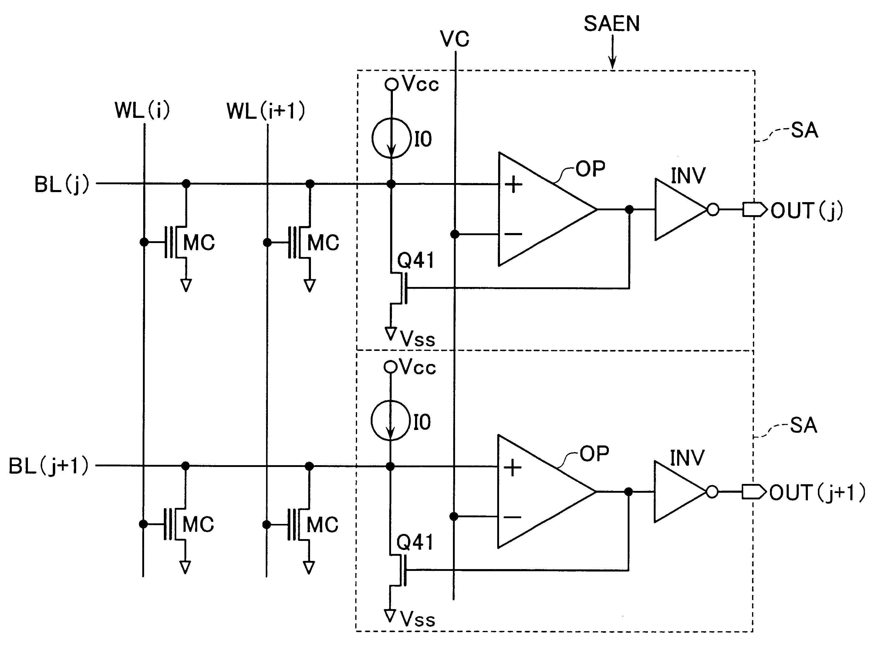
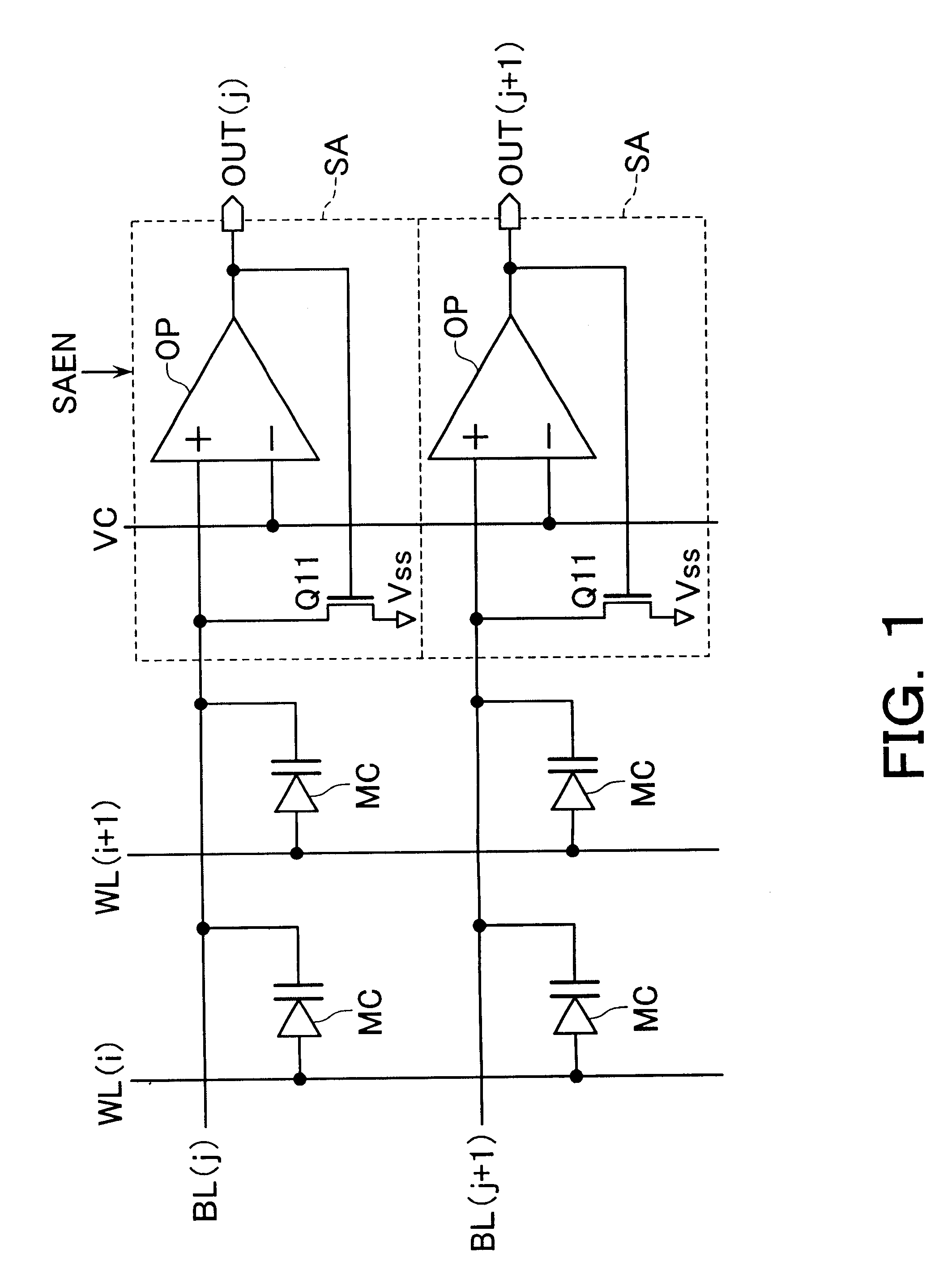
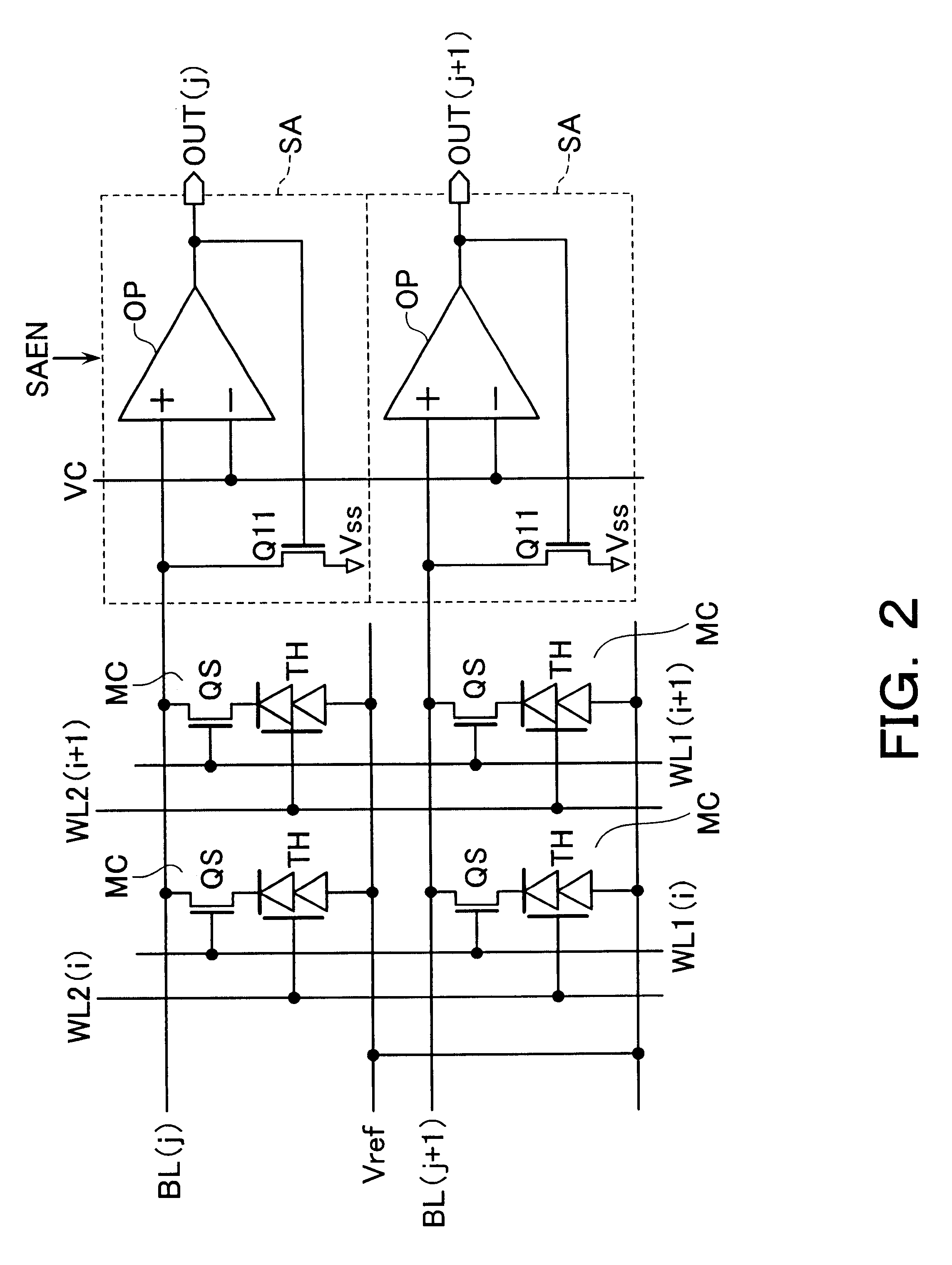
A sense amplifier scheme incorporating the principles of this invention is such that an operational amplifier and clamping circuit are used to enable execution of control for forcing the bit line of interest to stay at a constant or "fixed" potential level without regard to data being presently read. Accordingly, unlike the prior art schemes for determination of a bit-line clamp potential through ratio operations in the way stated in the introductory part of the description, it is possible to suppress or minimize stresses of current-driven memory cells to thereby obtain much increased read-out margins.

Memory cells to which the sense amplifiers embodying this invention are the so-called current-driven memory cells, typically including (a) memory cells of the type functioning to flow out or "push" a current toward a bit line(s) in a way conformity with data when selection, and (b) cells of the type acting to draw thereinto or "pull in" a current in accordance with data when selected.

S...


PUM


Abstract

An integrated semiconductor memory device with an array of memory cells MC using magnetic tunnel junction (MTJ) cells is disclosed. A sense amplifier SA that is connected to a bit line BL for data readout of a selected memory cell MC is arranged using an operational amplifier OP. The operational amplifier OP has an inverting input terminal which is connected to the bit line BL and a non-inverting input terminal, to which a potentially fixed constant voltage VC is given. A PMOS transistor Q31 is provided, which can also do double-duty as a current source load. This PMOS transistor has its drain and gate that are connected to the inverting input terminal, and a source as connected to an output terminal of the operational amplifier OP whereby the transistor is under feedback control in response to an output of the operational amplifier OP so that a clamped voltage potential of the bit lime BL is fixed to the voltage VC.

Description

This application is based on and claims the benefit of priority from prior Japanese Patent Application No. 2000-351787, filed on Nov. 17, 2000, the entire contents of which are incorporated herein by reference.1. Field of the InventionThis invention relates to semiconductor memory integrated circuit (IC) devices configured using memory cells of the current readout type.2. Description of Related ArtCurrently available memory cells adaptable for use in semiconductor memory IC devices include those cells of the type performing data storage depending upon whether a current flowing during cell selection is present or absent or alternatively whether such current is large or small in amount. This type of memory cells will be referred to hereinafter as the "current-driven" type memory cells in the description. Known current-driven memory cells include non-volatile memory cells suitable for use with electrically programmable read-only memory (EPROM) and electrically erasable programmable rea...

Claims


Application Information

Patent Timeline
Patent Type & Authority Patents(United States)
IPC IPC(8): G11C11/15G11C11/02H01L21/70H01L21/8246H01L27/22G11C11/56
CPCB82Y10/00G11C11/15G11C11/5607
Inventor IWATA, YOSHIHISA
Owner KK TOSHIBA
Why Eureka
Try Eureka