Processing method and apparatus using laser beam

Inactive Publication Date: 2006-11-09
DISCO CORP
View PDF19 Cites 6 Cited by
  • Summary
  • Abstract
  • Description
  • Claims
  • Application Information

AI Technical Summary

Benefits of technology

[0005] It is a principal object of the present invention, therefore, to provide a processing method and apparatus using a laser beam, which can expel as much debris, produced upon application of the laser beam, as possible out of the semiconductor wafer to minimize the debris remaining on the side surfaces of the grooves, thereby avoiding or suppressing the generation of heat distortion due to the debris, and thus sufficiently avoiding or suppressing the decrease in the deflective strength of the workpiece.
[0011] According to the processing method and apparatus of the present invention, the workpiece is melted by the application of the first laser beam and the second laser beam in the superposed state. Debris, which has been formed by the melting and is about to adhere to and remain on the side surfaces of the grooves, is expelled out of the grooves by the action of a widthwise outward portion of the second laser beam present beyond the width of the beam spot of the first laser beam. Thus, heat distortion due to remaining debris is avoided or suppressed. Consequently, the decrease in the deflective strength of the workpiece is fully avoided or suppressed.

Problems solved by technology

According to experiments conducted by the inventors, however, if the semiconductor wafer is divided to produce the individual semiconductor circuits by the above-described processing methods and apparatuses using a laser beam, the deflective strength of the products is relatively low.
According to the conventional processing methods and apparatuses, so-called debris generated by melting is not fully removed from the workpiece, but adheres to and remains on the side surfaces of the resulting grooves, with the result that heat distortion due to heat transmitted from the debris is caused to the neighborhood of the grooves.

Method used


Image

  • Processing method and apparatus using laser beam
  • Processing method and apparatus using laser beam
  • Processing method and apparatus using laser beam

Examples


Embodiment Construction

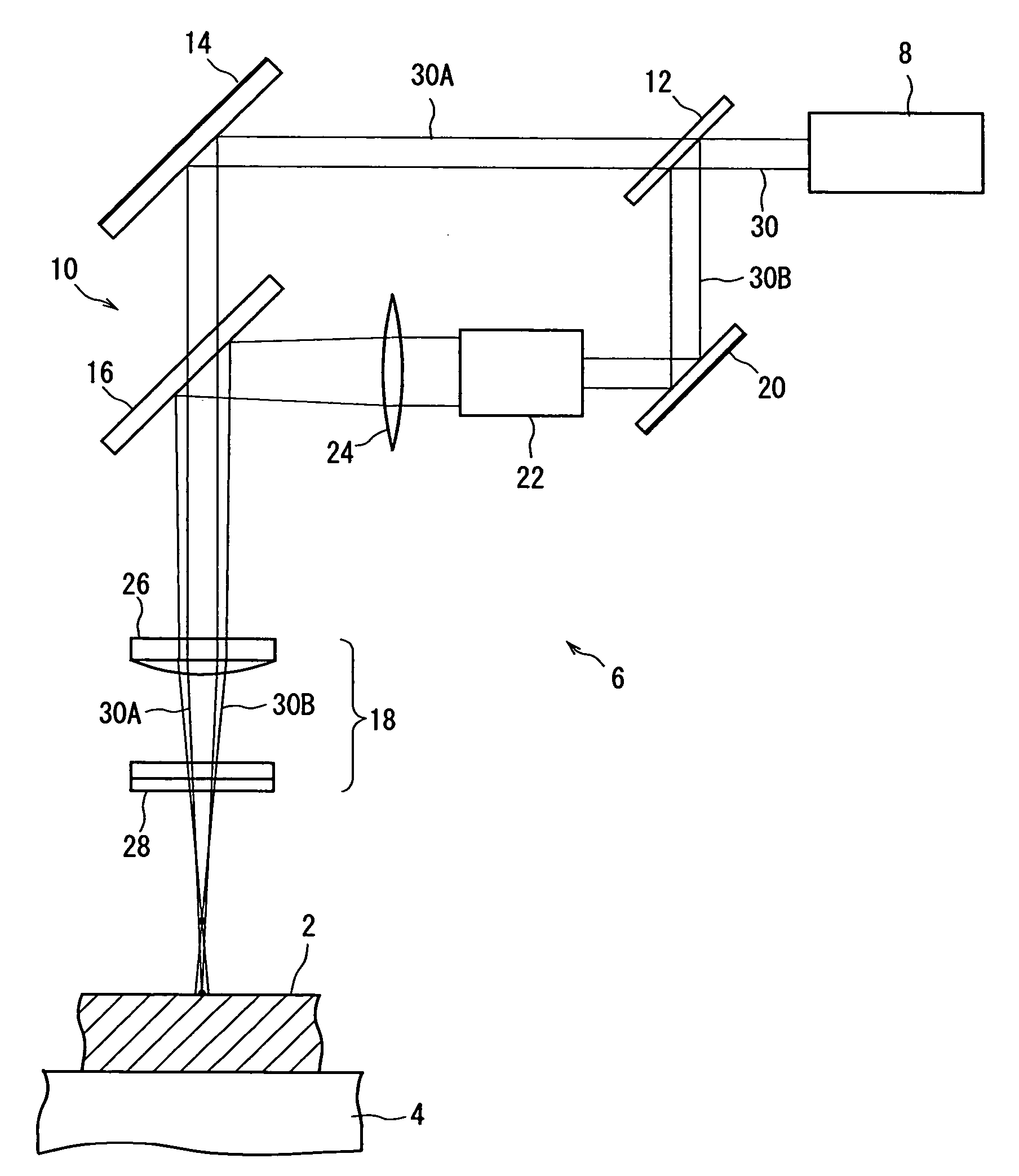
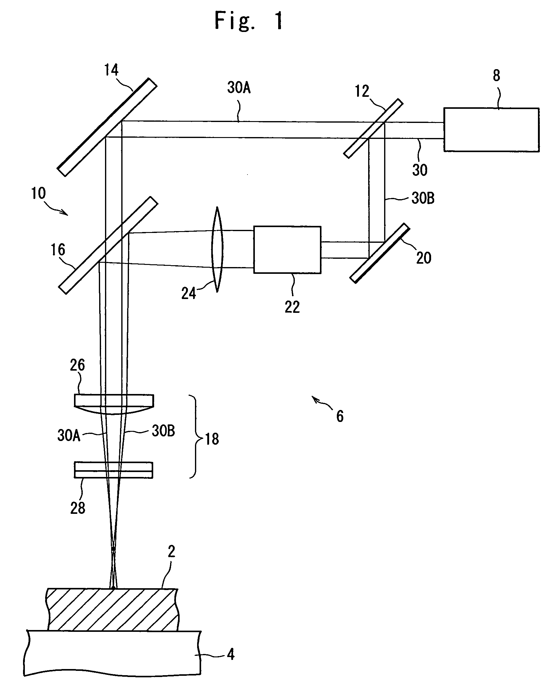
[0017] Preferred embodiments of the processing method and apparatus constituted in accordance with the present invention will be described in further detail by reference to the accompanying drawings.

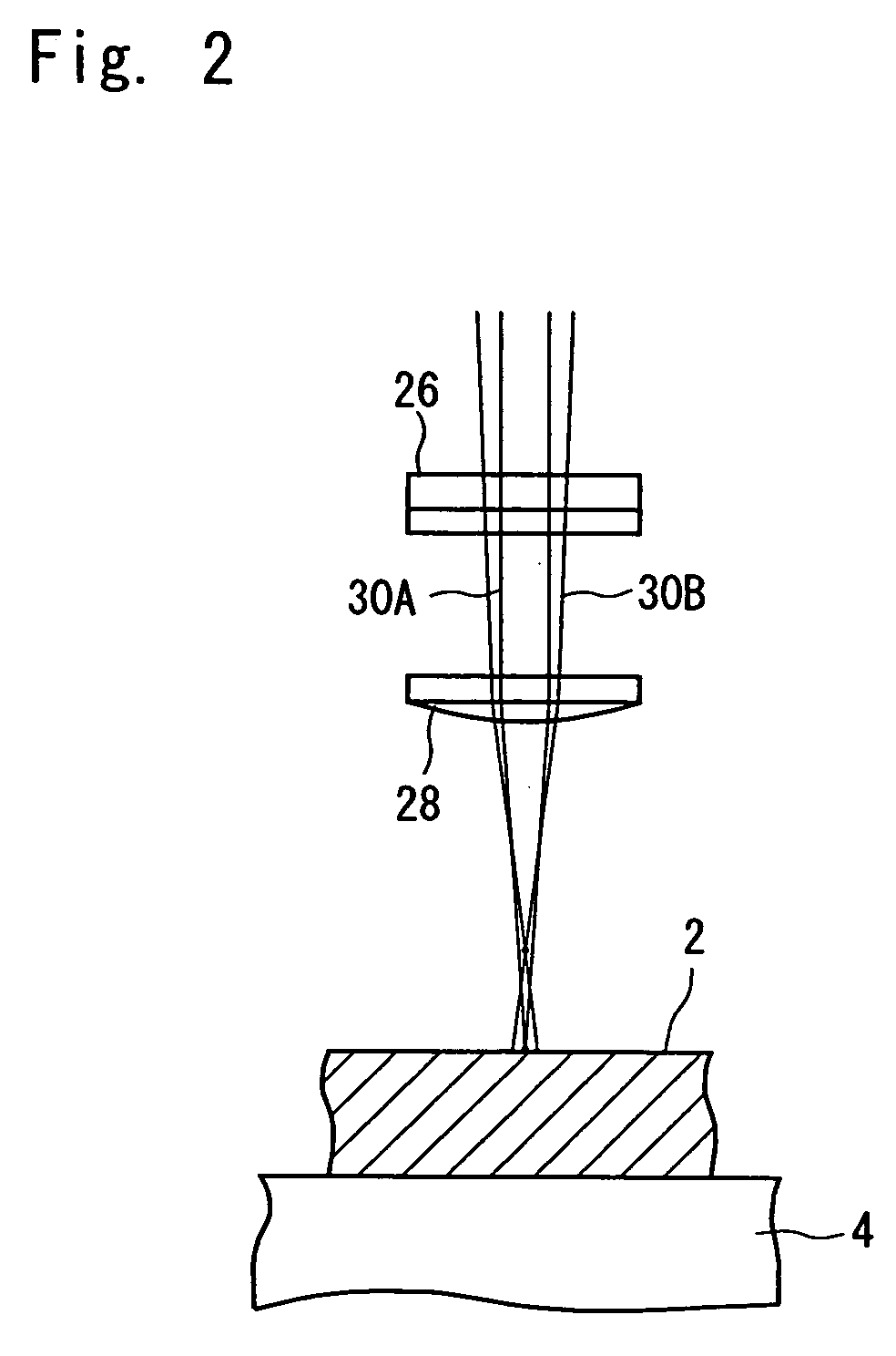
[0018]FIG. 1 schematically shows the preferred embodiment of the processing apparatus constructed according to the present invention. The illustrated processing apparatus is composed of a holding means 4 for holding a workpiece 2 such as a semiconductor wafer, and a laser beam application means indicated entirely at the numeral 6. The holding means 4 may be a vacuum attraction chuck which is composed of, for example, a porous member or a member having a plurality of suction holes and / or grooves, and which is brought into selective communication with a vacuum source (not shown). The holding means 4 is moved by a suitable drive means (not shown) in a right-and-left direction in FIG. 1 and a direction perpendicular to the sheet face of FIG. 1, and is also rotated about the axis of rotation...


PUM

PropertyMeasurementUnit
Currentaaaaaaaaaa
Digital informationaaaaaaaaaa
Diameteraaaaaaaaaa

Abstract

A processing method and apparatus using a laser beam, which can expel as much debris, produced upon application of a laser beam, as possible out of a workpiece to minimize the debris remaining on side surfaces of grooves. The processing method and apparatus superpose a first laser beam (30A) having a width D1 of a focal spot, and a second laser beam (30B) having a focal spot (32B) upstream, in a beam advancing direction, of the focal spot of the first laser beam, and having a width D2 of a beam spot at the focal spot of the first laser beam, D2 being larger than D1 (D2>D1); and apply the superposed laser beams to the workpiece.

Description

FIELD OF THE INVENTION [0001] This invention relates to a processing method and apparatus using a laser beam and, more particularly, a processing method and apparatus which move a workpiece, such as a semiconductor wafer, and a laser beam relative to each other while applying the laser beam to the workpiece. DESCRIPTION OF THE PRIOR ART [0002] In the production of a semiconductor device, for example, it is well known that many rectangular regions are defined by streets arranged in a lattice pattern on the face of a semiconductor wafer including a substrate, such as a silicon substrate, a sapphire substrate, a silicon carbide substrate, a lithium tantalate substrate, a glass substrate, or a quartz substrate, and a semiconductor circuit is formed in each of such rectangular regions. Then, the semiconductor wafer is divided along the streets to obtain the individual semiconductor circuits. [0003] As methods and apparatuses for dividing the semiconductor wafer along the streets, process...

Claims


Application Information

Patent Timeline
IPC IPC(8): B23K26/08B23K26/067
CPCB23K26/0604B23K26/367B23K26/16B23K26/0608B23K26/364
Inventor MORIKAZU, HIROSHIOGOSHI, NOBUMORITAKEYAMA, KOICHI
Owner DISCO CORP
Why Eureka
Try Eureka