Supercharge Your Innovation With Domain-Expert AI Agents!

Multi-chip module and method of manufacture

a technology of multi-chip modules and manufacturing methods, applied in the direction of semiconductor devices, semiconductor/solid-state device details, electrical apparatus, etc., can solve the problems of pliable or springy second semiconductor chips that overhang the spacer, catastrophic device failure, and weakening the bond formed

Active Publication Date: 2006-11-09
SPANSION LLC
View PDF7 Cites 7 Cited by
  • Summary
  • Abstract
  • Description
  • Claims
  • Application Information

AI Technical Summary

Benefits of technology

[0032] By now it should be appreciated that a multi-chip module having vertically stacked semiconductor chips and a method for manufacturing the multi-chip module been provided. An advantage of multi-chip modules in accordance with the present invention is that it provides a means for decreasing vibration or bounce of regions of a semiconductor chip during a wirebonding process. This improves the reliability of the wirebonds and decreases catastrophic device failure. Another advantage of the present invention is that it increases the variety in the sizes of the semiconductor chips that can be bonded to a spacer. Because the support material provides additional support for the semiconductor chip, larger chips can be mounted to the spacer. In addition, the method is readily integrable into multi-chip module processing flows in a cost and time efficient manner.

Problems solved by technology

A drawback with this type of structure is that the portions of the second semiconductor chip that overhang the spacer are pliable or springy.
Thus, when the bonding pads located on the overhanging portion of the second semiconductor chip are wirebonded to the corresponding bonding pads located on the circuit board, the pliability of the overhanging portions of the second semiconductor chip weakens the bonds formed to bonding pads on the second semiconductor chip.
This bond weakening causes catastrophic device failure.

Method used


Image

  • Multi-chip module and method of manufacture
  • Multi-chip module and method of manufacture
  • Multi-chip module and method of manufacture

Examples


Embodiment Construction

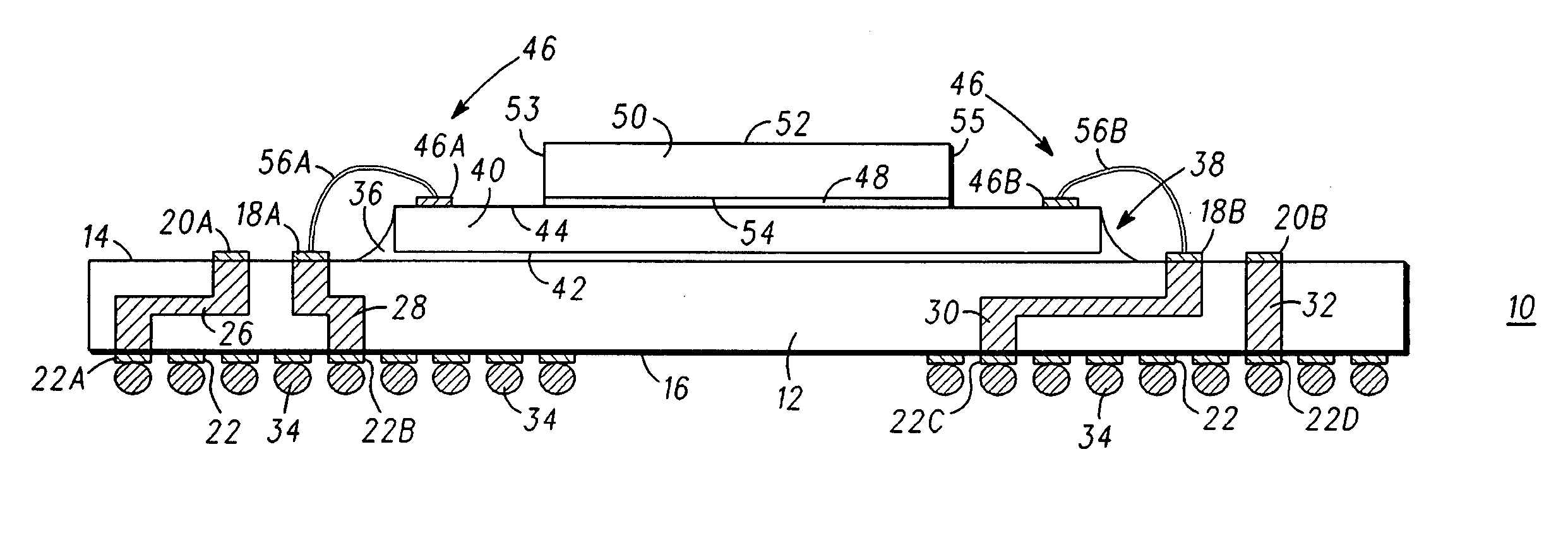
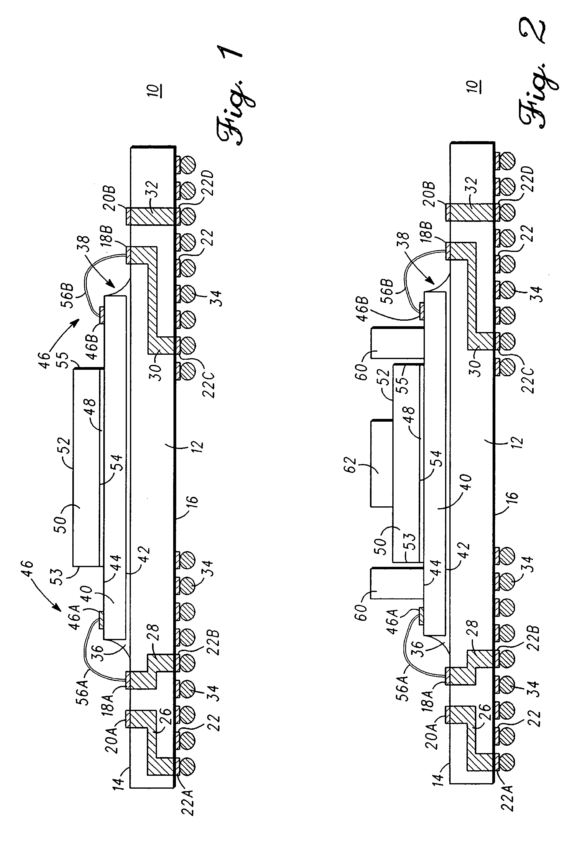
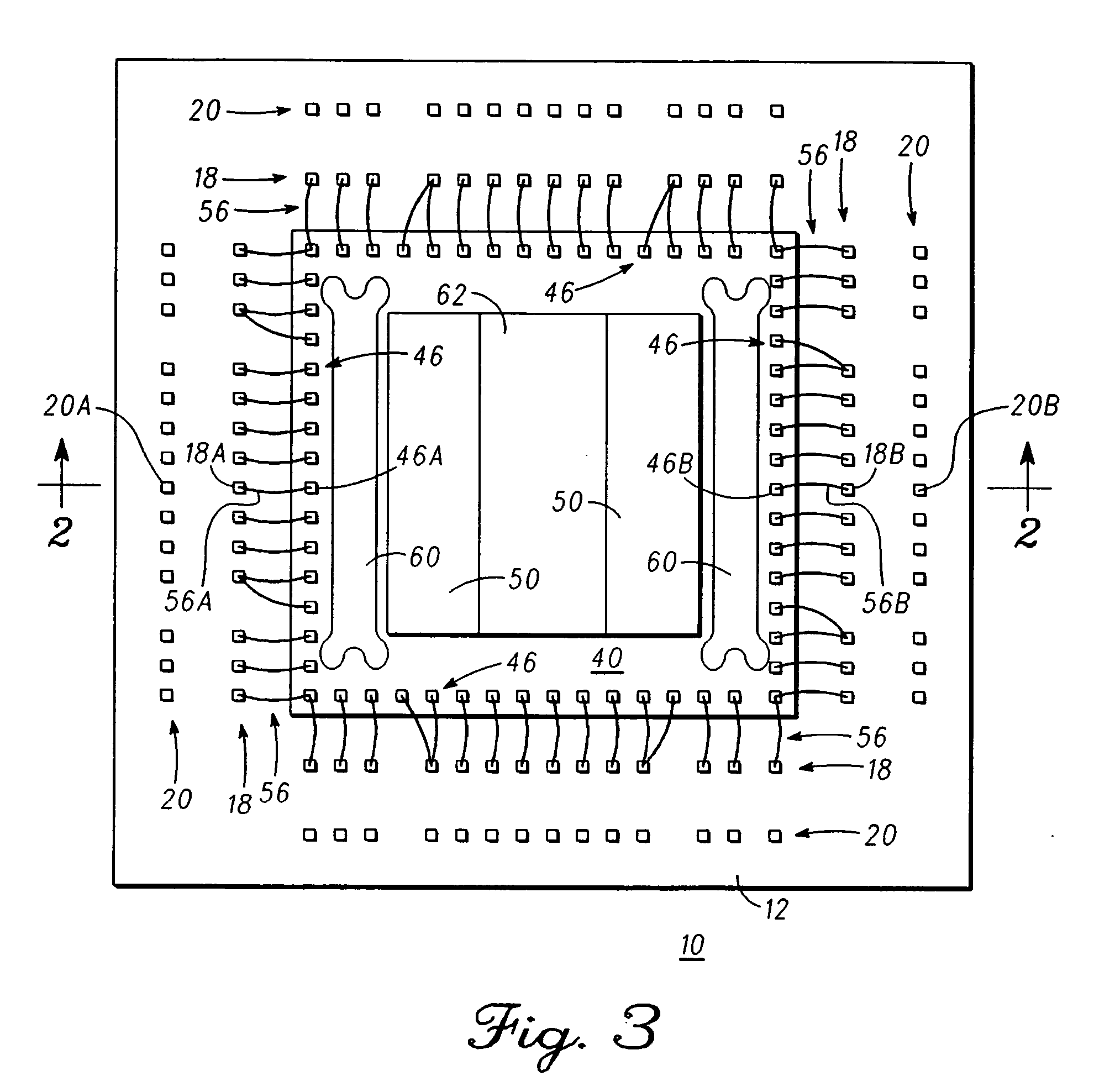
[0017] Generally, the present invention provides a multi-chip module and a method for manufacturing the multi-chip module, wherein the semiconductor chips of the multi-chip module are vertically stacked. In vertically stacking the semiconductor chips of a multi-chip module, a spacer is inserted between the semiconductor chips to allow clearance for the wirebonds. A portion of the semiconductor chip positioned above the spacer overhangs the edges of the spacer. The portions of a semiconductor chip overhanging the spacer are pliable. Although the pliability increases the fragility of semiconductor chips in general, the increased fragility is more pronounced in semiconductor chips having thicknesses of less than about 0.6 millimeters (mm). This pliability allows the semiconductor chip to vibrate during the wirebonding process, which breaks the wires being bonded to bonding pads on the semiconductor chip. In accordance with the present invention, the vibration is mitigated by forming a ...


PUM


Abstract

A multi-chip module and a method for manufacturing the multi-chip module that mitigates wire breakage. A first semiconductor chip is mounted and wirebonded to a support substrate. A spacer is coupled to the first semiconductor chip. A support material is disposed on the spacer and a second semiconductor chip is positioned on the support material. The second semiconductor chip is pressed into the support material squeezing it into a region adjacent the spacer and between the first and second semiconductor chips. Alternatively, the support material is disposed on the first semiconductor chip and a die attach material is disposed on the spacer. The second semiconductor chip is pressed into the die attach material and the support material, squeezing a portion of the support material over the spacer edges. Wirebonds are formed between the support substrate and the first and second semiconductor chips.

Description

FIELD OF THE INVENTION [0001] The present invention relates, in general, to semiconductor components and, more particularly, to semiconductor components comprising multi-chip modules. BACKGROUND OF THE INVENTION [0002] The desire for faster, cheaper, and more efficient semiconductor components has motivated semiconductor component manufacturers to shrink the sizes of the devices fabricated in a semiconductor chip and place multiple semiconductor chips in a single package typically referred to as a multi-chip module. The semiconductor chips in a multi-chip module can be placed either in a horizontal orientation, i.e., beside each other, or in a vertical orientation, i.e., vertically stacked on top of each other. In a conventional vertically stacked multi-chip module, a first semiconductor chip is attached to a circuit board by adhesive bonding followed by wirebonding bonding pads located on the semiconductor chip to corresponding bonding pads located on the circuit board. A spacer is...

Claims


Application Information

Patent Timeline
Patent Type & Authority Applications(United States)
IPC IPC(8): H01L29/74
CPCH01L25/0657H01L25/065H01L2224/48091H01L2224/48227H01L2225/0651H01L2225/06575H01L2225/06593H01L2924/09701H01L2924/15184H01L2924/15311H01L2924/16152H01L2924/3025H01L25/50H01L2924/01087H01L2924/00014H01L23/12
Inventor FOONG, YIN LYEKEE, CHENG SIMLEE, LAY HONGABU-HASSAN, MOHAMED SUHAIZAL BIN
Owner SPANSION LLC
Features
  • R&D
  • Intellectual Property
  • Life Sciences
  • Materials
  • Tech Scout
  • Unparalleled Data Quality
  • Higher Quality Content
  • 60% Fewer Hallucinations
Learn More