
Optical information storage unit
a technology of information storage and optical media, applied in the field of information storage units, can solve the problems of large power consumption, high cost, and high cost of solid-state memories, and achieve the effect of high information storage capacity per unit area
- Summary
- Abstract
- Description
- Claims
- Application Information
AI Technical Summary
Benefits of technology
Problems solved by technology
Method used
Image

Examples
first embodiment
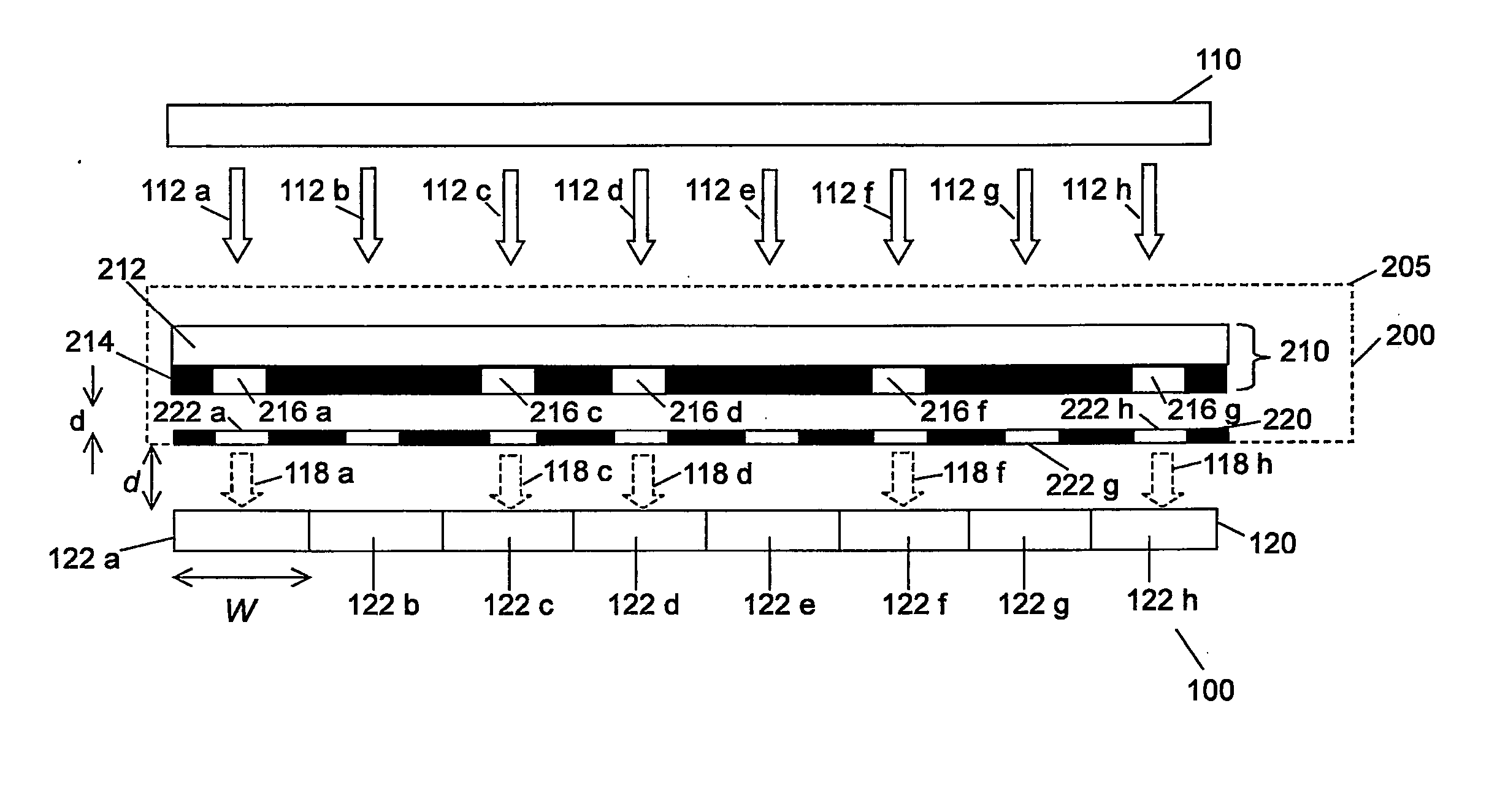
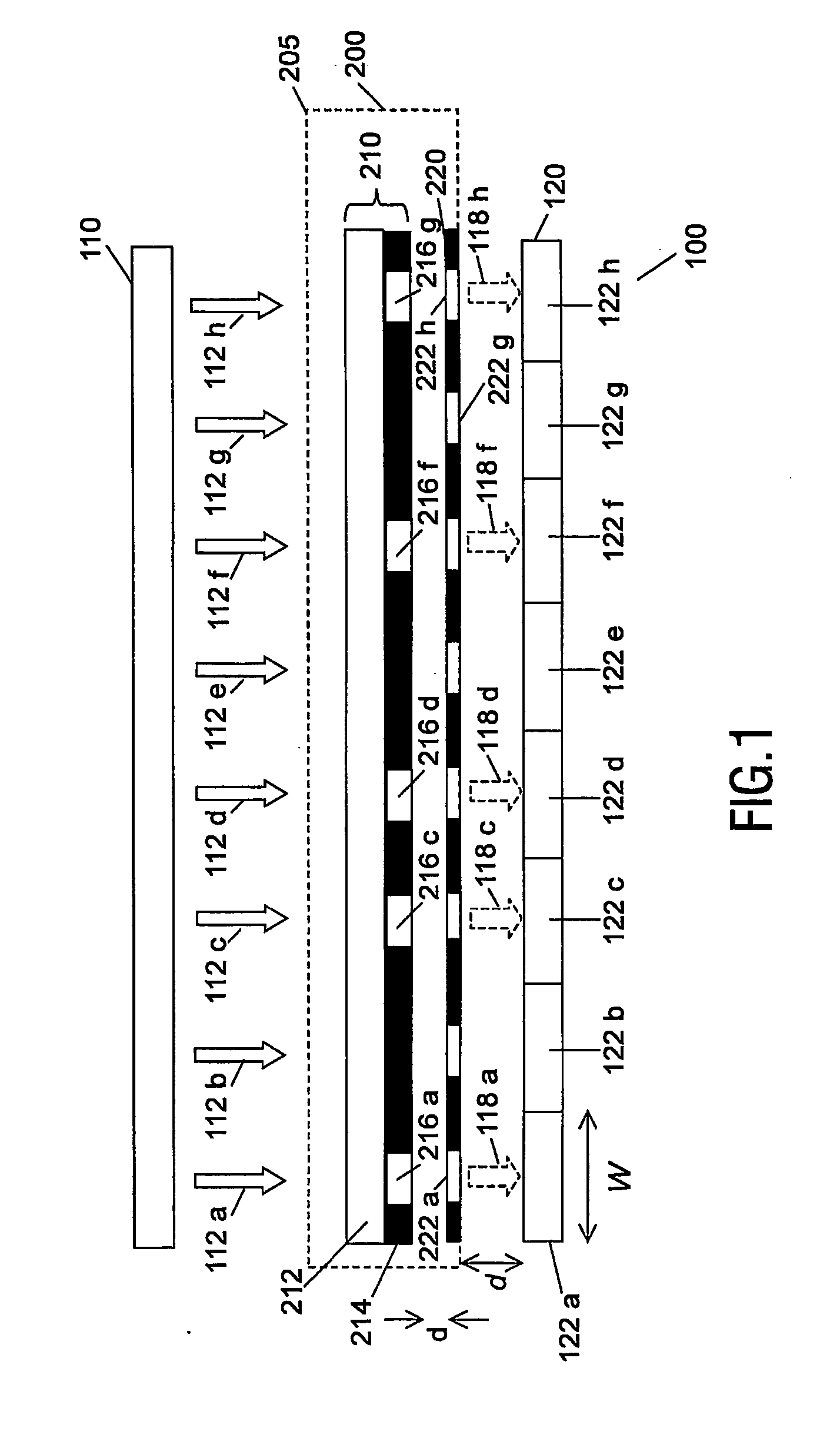
[0027]FIG. 1 shows a cross sectional view of an optical information storage unit 200 within a reader 100.
[0028] The information storage unit 200 in this instance is a removable optical memory card. The card consists of a sealed but optically transparent cartridge 205 enclosing an information layer 210 and a readout layer 220.
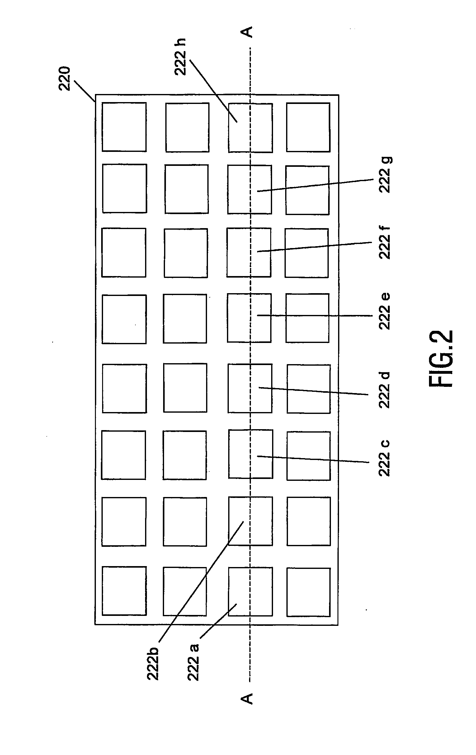
[0029]FIG. 2 shows a plan view of the readout layer 220, and FIG. 3 shows a plan view of the information layer 210. In FIGS. 2 and 3, the dotted line AA indicates the plane of the cross sectional view shown in FIG. 1.
[0030] The readout layer 220 comprises an optically opaque substrate. An array of optical apertures (e.g. 222a, 222b, . . . 222h) is provided, the apertures allowing light to be transmitted through the readout layer 220.
[0031] The information layer 210 in this instance comprises a transparent layer 212 overlaid by an optically opaque covering layer 214. The transparent layer 212 is used to supply mechanical strength to the information layer 210, ...
third embodiment
[0050]FIG. 5 illustrates a cross sectional view of a card and a reader in accordance with the present invention.
[0051] It will be observed that the card 1200 comprises an information layer 1210 and a readout layer 1220. As previously, the information layer 1210 comprises a transparent layer 1212 and an optically opaque layer 1214.
[0052] The reader 100 comprises a light source 110 and an optical sensor 120. The optical sensor comprises an array of light sensing areas, each area being of width W.
[0053] The readout layer comprises a plurality of apertures (1222a, 1222b, 1222c, . . . ), with one aperture per width W of the readout layer. In this particular embodiment, the overall width of the optical sensor 120 is the same as the overall width of the readout layer 1220, such that each aperture in the readout layer corresponds to a respective light sensing area (122a, 122b, 122c, . . . ) of the optical sensor 120.
[0054] The significant difference between this particular embodiment and...
PUM
 Abstract
Description
Claims
Application Information