Clock design apparatus and clock design method

a clock design and clock technology, applied in the field of clock wiring technology, can solve the problem of not reducing the clock skew

Inactive Publication Date: 2006-11-09
KK TOSHIBA
View PDF10 Cites 16 Cited by
  • Summary
  • Abstract
  • Description
  • Claims
  • Application Information

AI Technical Summary

Benefits of technology

[0008] According to an aspect of the invention, a clock design apparatus includes a delay time adjusting section, a prohibition specifying section and a clock tree synthesis section. The delay time adjusting section is configured to adjust signal delay time of signal propagation paths on a semiconductor integrated circuit to be designed

Problems solved by technology

However, the method disclosed in JP Hei. 7-98617 can cope with variations in the manufacture, but cannot

Method used


Image

  • Clock design apparatus and clock design method
  • Clock design apparatus and clock design method
  • Clock design apparatus and clock design method

Examples


first embodiment

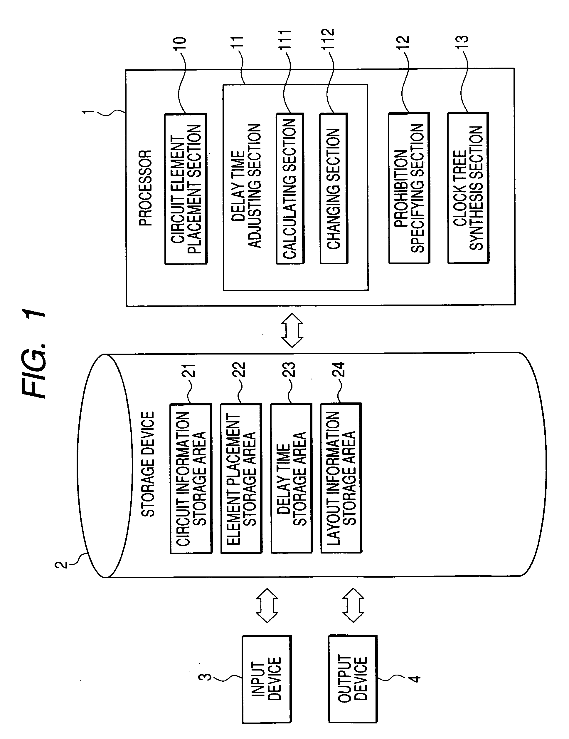
[0027] A clock design apparatus according to a first embodiment of the invention includes a delay time adjusting section 11, a prohibition specifying section 12 and a clock tree synthesis section 13 as shown in FIG. 1. The delay time adjusting section 11 adjusts a signal delay time of a signal propagation path on a semiconductor integrated circuit to be designed. The prohibition specifying section 12 specifies a part of the signal propagation path as a circuit prohibited from being changed. The clock tree synthesis section 13 synthesizes a clock tree of the semiconductor integrated circuit in accordance with the specification made by the prohibition specifying section 12. The clock tree synthesis process is hereinafter referred to as a “CTS process”.

[0028] The delay time adjusting section 11 includes a calculating section 111 and a changing section 112. The calculating section 111 calculates the signal delay time of the signal propagation path, based on circuit information of the s...

second embodiment

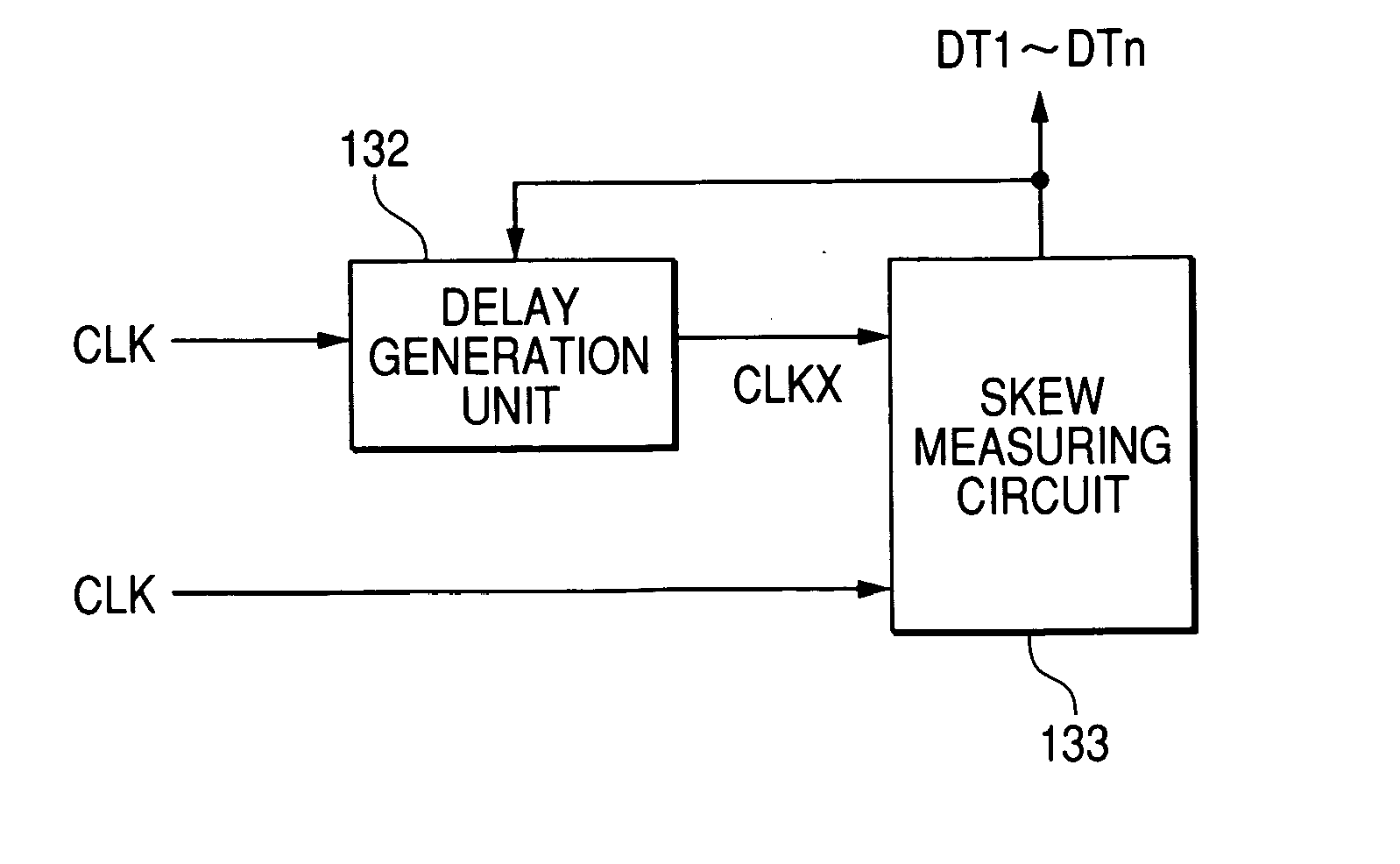
[0074] A clock design apparatus according to a second embodiment of the invention is different from that of FIG. 1 in that it further comprises a fixed-delay-circuit adjusting section 15, as shown in FIG. 13. The other configuration is the same as the first embodiment shown in FIG. 1. The fixed-delay-circuit adjusting section 15 adjusts the signal delay time in each of plural fixed delay generation units contained in the semiconductor integrated circuit.

[0075] The fixed-delay-circuit adjusting section 15 includes a delay calculating section 1501 and a circuit changing section 1502. The delay calculating section 1501 calculates the signal delay time of a fixed delay generation unit. The circuit changing section 1502 changes the fixed delay generation unit by inserting a buffer circuit.

[0076] An automatic clock design method for the semiconductor integrated circuit, which is performed by the clock design apparatus shown in FIG. 13, will be described below illustratively, using the s...


PUM


Abstract

A clock design apparatus includes a delay time adjusting section, a prohibition specifying section and a clock tree synthesis section. The delay time adjusting section is configured to adjust signal delay time of signal propagation paths on a semiconductor integrated circuit to be designed. The prohibition specifying section is configured to specify a part of the signal propagation paths as a circuit prevented from being changed. The clock tree synthesis section is configured to synthesize a clock tree of the semiconductor integrated circuit in accordance with the specification made by the prohibition specifying section.

Description

CROSS-REFERENCE TO RELATED APPLICATIONS [0001] This application is based upon and claims the benefit of priority from the Japanese Patent Application No. 2005-116208 filed on Apr. 13, 2005; the entire contents of which are incorporated herein by reference. BACKGROUND OF THE INVENTION [0002] 1. Field of the Invention [0003] The invention relates to a clock wiring technology, and more particularly to a clock design apparatus and a clock design method for designing the clock wiring of a semiconductor integrated circuit in which its clock frequency and supply voltage are changed. [0004] 2. Description of the Related Art [0005] A method for realizing the lower power consumption of a semiconductor integrated circuit by changing the clock frequency and the supply voltage of a logical block in the semiconductor integrated circuit according to the workload has been in practical use. This method is characterized by changing the clock frequency and the supply voltage of the logical block to be...

Claims


Application Information

Patent Timeline
IPC IPC(8): G06F17/50
CPCG06F17/505G06F2217/78G06F2217/62G06F17/5077G06F30/327G06F30/396G06F30/394G06F2119/06
Inventor KITAHARA, TAKESHITSUKIBOSHI, YOSHIKI
Owner KK TOSHIBA
Why Eureka
Try Eureka