Dry etching method, fabrication method for semiconductor device, and dry etching apparatus

a technology of dry etching and fabrication method, which is applied in the direction of electrical equipment, decorative arts, electric discharge tubes, etc., can solve the problems of inability to form the desired isolation depth of the trench, the difficulty of providing a sufficient active region having a sufficient size, and the degrade of the electric characteristics of the semiconductor devi

Inactive Publication Date: 2006-11-16
TAIWAN SEMICON MFG CO LTD
View PDF22 Cites 1 Cited by
  • Summary
  • Abstract
  • Description
  • Claims
  • Application Information

AI Technical Summary

Benefits of technology

[0069] In the dry etching apparatus of the present invention, the source power applying means initiates the application of the source power when the time elapsed from the time at which the bias power applying means initiates the application of the bias power reaches the specified time. In short, the application of the bias power is inevitably initiated before the application of the source power is initiated. Even if etching is performed with respect to the silicon-containing material as the object to be etched by using a process gas containing oxygen, therefore, t

Problems solved by technology

As feature sizes have been reduced increasingly, however, the problem has arisen that the isolation is larger than a desired size, which makes it difficult to provide an active region having a sufficient size.
If a trench for isolation is formed in a silicon substrate by using the conventional dry etching method, e.g., however, etching is halted halfway, as shown in FIG. 14, which leads to the problem that the trench for isolation having a desired isolation depth cannot be formed. FIG. 14 shows the state in which etching has been halted halfway in the dry etching step shown in FIG. 11C.
If the conventional dry etching method is used for a silicon substrate or

Method used


Image

  • Dry etching method, fabrication method for semiconductor device, and dry etching apparatus
  • Dry etching method, fabrication method for semiconductor device, and dry etching apparatus
  • Dry etching method, fabrication method for semiconductor device, and dry etching apparatus

Examples


embodiment 1

[0087] Referring now to the drawings, a method for fabricating a semiconductor device according to a first embodiment of the present invention will be described.

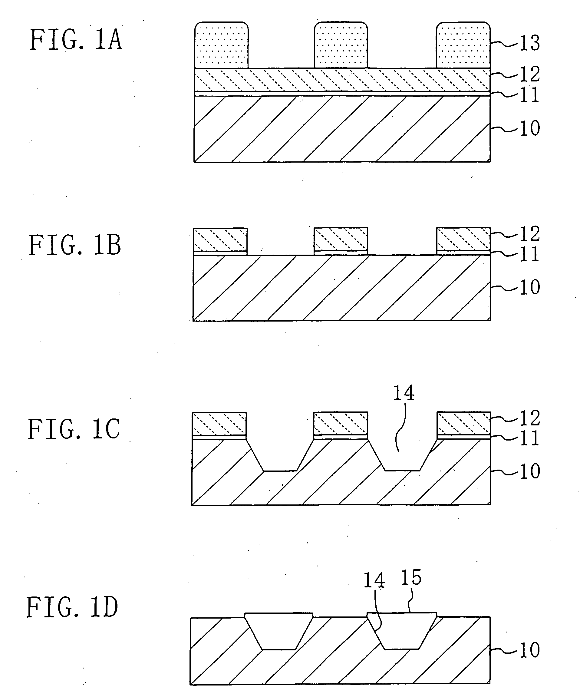
[0088]FIGS. 1A to 1D are cross-sectional views illustrating the individual process steps of the method for fabricating a semiconductor device according to the first embodiment.

[0089] First, as shown in FIG. 1A, a silicon oxide film 11 is formed on a silicon substrate 10 by, e.g., thermal oxidation, followed by a silicon nitride film 12 formed on the first silicon oxide film 11 by using a film forming method such as CVD. Then, a resist pattern 13 having openings each corresponding to a region to be formed with an isolation is formed on the silicon nitride film 12 by photolithography.

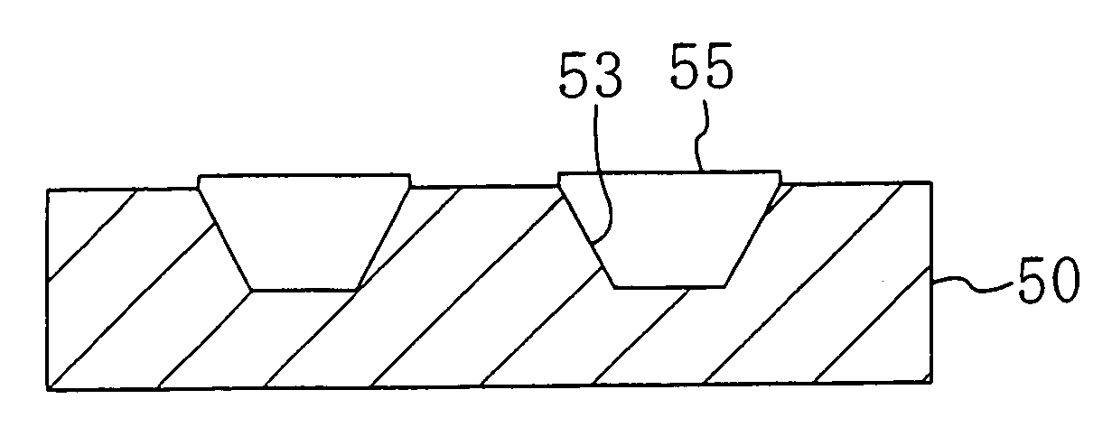
[0090] Next, as shown in FIG. 1B, dry etching is performed with respect to the silicon nitride film 12 and to the first silicon oxide film 11 by using the resist pattern 13 as a mask, thereby pattering each of the silicon nitride film 12 and th...

embodiment 2

[0102] A method for fabricating a semiconductor device according to a second embodiment of the present invention will be described with reference to the drawings.

[0103]FIGS. 5A to 5C are cross-sectional views illustrating the individual process steps of the method for fabricating a semiconductor device according to the second embodiment.

[0104] First, as shown in FIG. 5A, a gate insulating film 21 composed of a silicon oxide film is formed on a silicon substrate 20 by thermal oxidation, followed by a polysilicon film 22 formed on the gate insulating film 21 by using a film forming method such as CVD. Then, a resist pattern 23 covering a region to be formed with a gate electrode is formed on the polysilicon film 22 by photolithography.

[0105] Next, as shown in FIG. 5B, dry etching is performed with respect to the polysilicon film 22 masked with the resist pattern 23, thereby forming a gate electrode 24 composed of the polysilicon film 22 on the silicon substrate 20 with the gate ins...

embodiment 3

[0113] A method for fabricating a semiconductor device according to a third embodiment of the present invention will be described with reference to the drawings.

[0114]FIGS. 6A to 6E are cross-sectional views illustrating the individual process steps of the method for fabricating a semiconductor device according to the third embodiment.

[0115] First, as shown in FIG. 6A, a first silicon oxide film 31 is formed on a silicon substrate 30 by, e.g., thermal oxidation, followed by a silicon nitride film 32 formed on the first silicon oxide film 31 by using a film forming method such as CVD. Then, a resist pattern (not shown) having openings each corresponding to a region to be formed with an isolation is formed on the silicon nitride film 32 by photolithography. Thereafter, dry etching is performed with respect to the silicon nitride film 32 and to the first silicon oxide film 31 by using the resist pattern as a mask, thereby patterning each of the silicon nitride film 32 and the first s...


PUM

PropertyMeasurementUnit
Poweraaaaaaaaaa
Speedaaaaaaaaaa
Electrical conductoraaaaaaaaaa

Abstract

When etching is performed with respect to a silicon-containing material by using a dry etching apparatus having a dual power source, the application of bias power is initiated before oxidization proceeds at a surface of the silicon-containing material. Specifically, the application of the bias power is initiated before the application of source power is initiated. Alternatively, the source power and the bias power are applied such that the effective value of the source power reaches a second predetermined value after the effective value of the bias power reaches a first predetermined value.

Description

BACKGROUND OF THE INVENTION [0001] The present invention relates to a dry etching method for a material containing silicon, a method for fabricating a semiconductor device using the dry etching method, and a dry etching apparatus for implementing the dry etching method. [0002] When dry etching is performed with respect to a material containing silicon (hereinafter referred to as the silicon-containing material) in the fabrication of a semiconductor device, a dry etching apparatus having a dual power source such as an inductively coupled plasma etching apparatus (ICP) has been used to miniaturize a semiconductor element and increase the precision thereof. The dry etching apparatus having the dual power source features separate and controlled application of first electric power (hereinafter referred to as source power) for generating a plasma of a process gas introduced into a chamber and adjusting the density of the plasma and second electric power (hereinafter referred to as bias po...

Claims


Application Information

Patent Timeline
IPC IPC(8): H01L21/76H01L21/00H01L21/3065
CPCH01J37/32H01J37/32706H01J2237/334H01L21/02057H01L21/02071H01L21/02238H01L21/76232H01L21/02255H01L21/3065H01L21/31662H01L21/32137H01L21/67069H01L21/02252
Inventor YAMASHITA, TAKESHIYAMAGUCHI, TAKAONIKO, HIDEO
Owner TAIWAN SEMICON MFG CO LTD
Why Eureka
Try Eureka