Image sensing apparatus

a technology image sensor, which is applied in the field of image sensing apparatus, can solve the problems of raising the production cost of the image sensing apparatus incorporated with the image sensor, and achieve the effect of preventing or suppressing the occurrence of inversion and simplifying the arrangemen

Inactive Publication Date: 2006-11-23
KONICA MINOLTA PHOTO IMAGING
View PDF3 Cites 29 Cited by
  • Summary
  • Abstract
  • Description
  • Claims
  • Application Information

AI Technical Summary

Benefits of technology

[0009] It is another object of the present invention to provide an image sensing apparatus which can prevent or suppress occurrence of inversion with a simplified arrangement.

Problems solved by technology

There is a case that an image sensing apparatus loaded with a CMOS image sensor may suffer from a phenomenon that an image area having a high luminance is captured in black.
In the publication, since the high luminance black crushing circuit is constituted of the capacitors, the switching devices, and the operation amplifiers to constantly monitor the reset levels or the second signals of the respective switching devices, the construction of the image sensor is complicated, which may raise the production cost of an image sensing apparatus incorporated with the image sensor.

Method used


Image

  • Image sensing apparatus
  • Image sensing apparatus
  • Image sensing apparatus

Examples


first embodiment

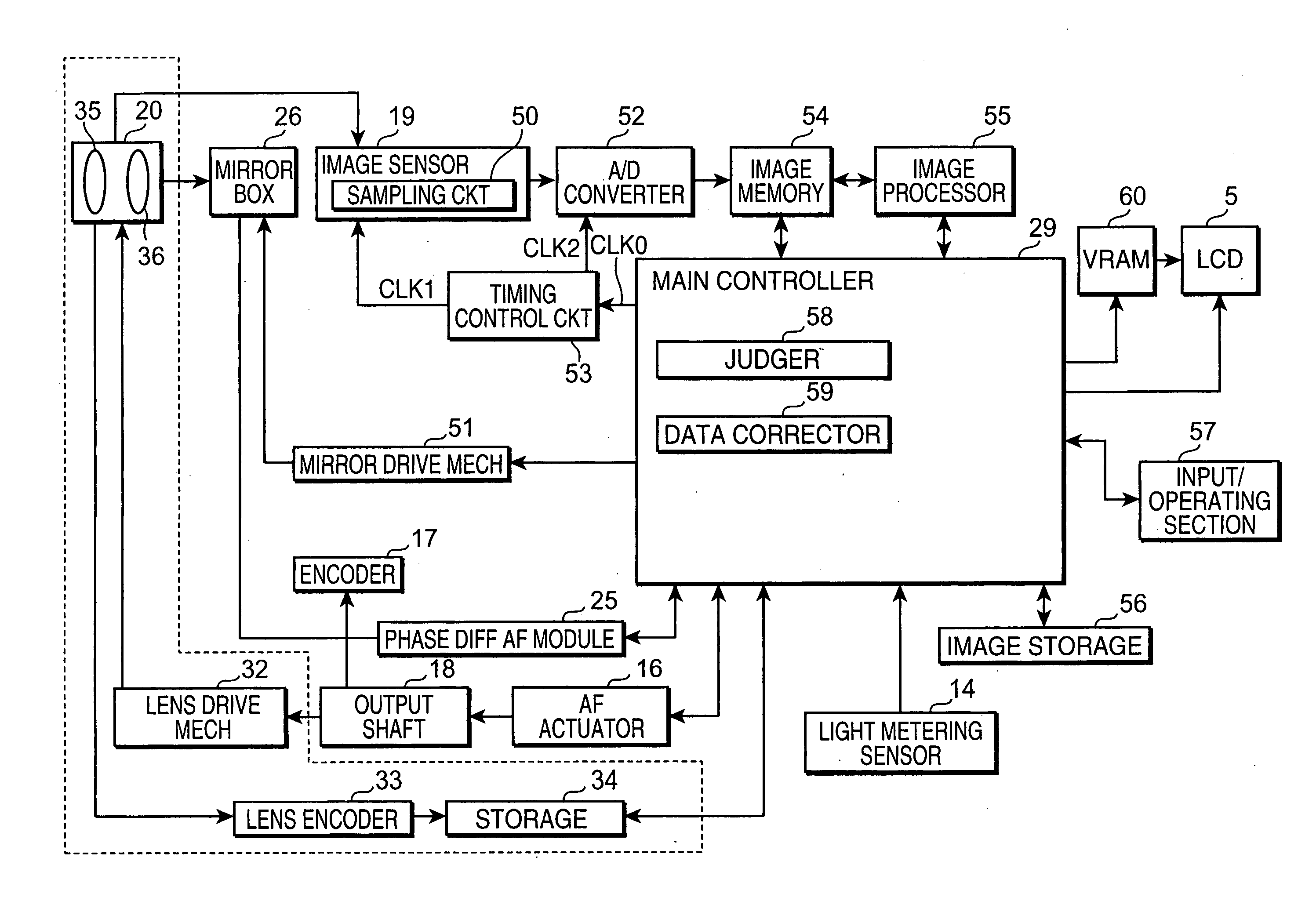
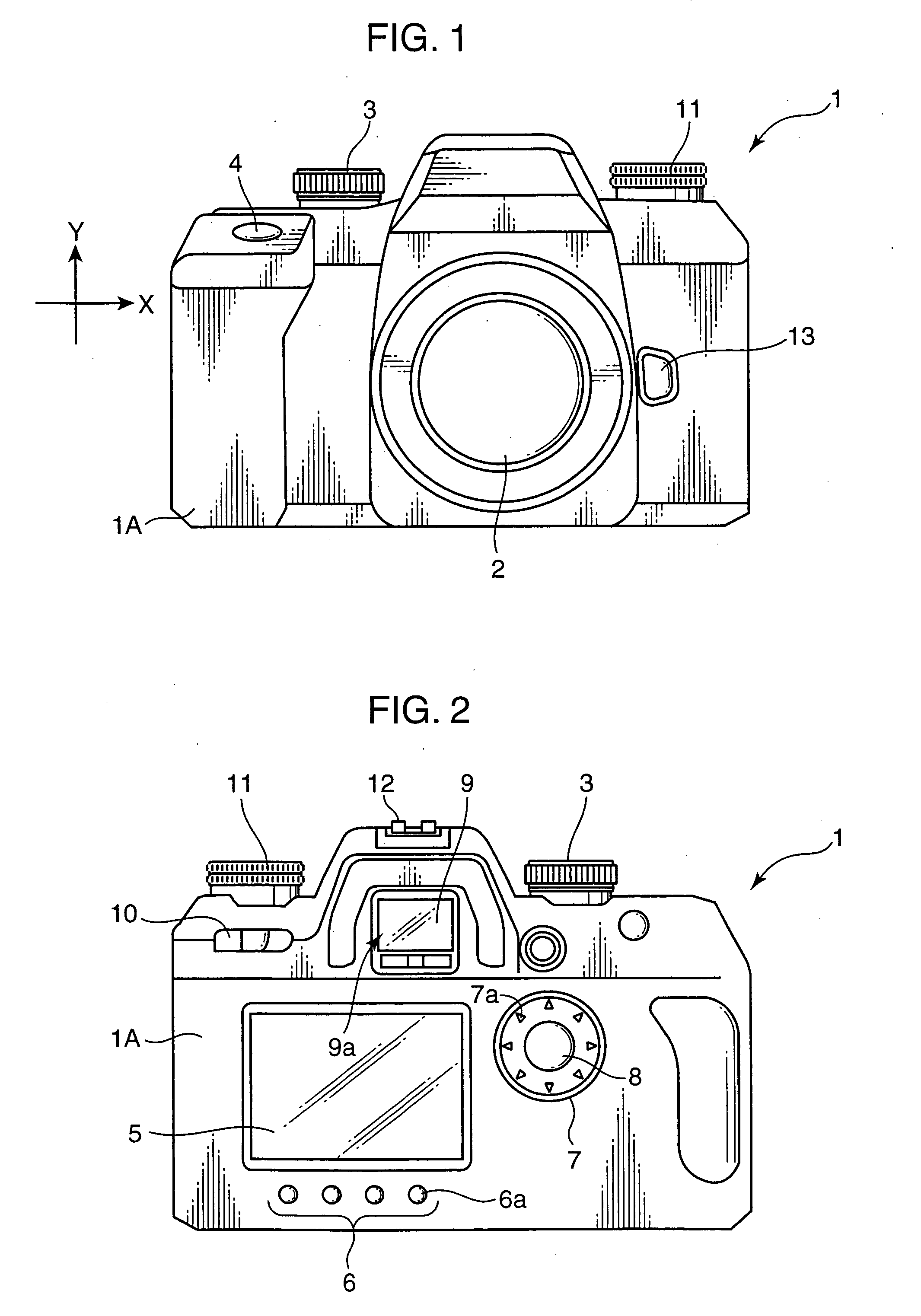
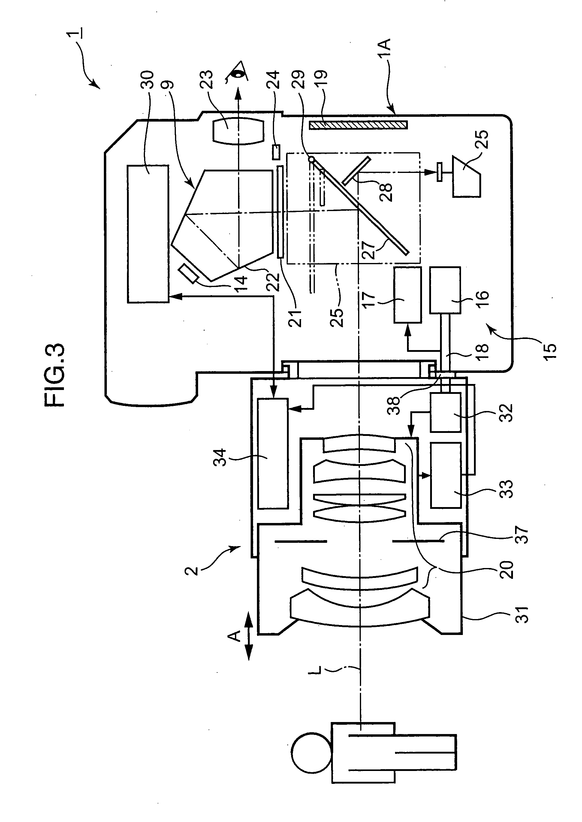
[0037] An image sensing apparatus embodying the invention will be described with reference to drawings. Elements identical to each other in the drawings are denoted at the same reference numerals. Referring to FIGS. 1 to 3 showing an image sensing apparatus in the invention, the image sensing apparatus 1 is a single lens reflex image sensing apparatus having a lens unit 2 exchangeably or detachably attached to a box-shaped apparatus body 1A.

[0038] The image sensing apparatus 1 comprises the lens unit 2 which is attached to a substantially middle part to a front face of the apparatus body 1A, a first mode setting dial 3 which is arranged at an appropriate position on an upper face of the apparatus body 1A, a shutter button 4 which is arranged at a corner portion on the upper face of the apparatus body 1A, a liquid crystal display (LCD) 5 which is arranged on a left side of a rear face of the apparatus body 1A in FIG. 2, a setting button group 6 which is arranged on a lower part relat...

second embodiment

[0164] In the second embodiment, the pixels are divided into pixels for use in judging whether there is a possibility of inversion, and pixels for use in generating a live-view image or a moving image. Alternatively, it is possible to judge whether there is a possibility of inversion and to generate a live-view image or a moving image without dividing the pixels by implementing the following processing.

[0165] As shown in FIG. 20, the main controller 123 or the image capture controller 124 divides each cycle of updating and displaying a live-view image into two periods, namely, a former half period corresponding to a second period, and a latter half period corresponding to a first period, for instance.

[0166] In this modification, in the case where it is judged that pixel data of a live-view image generation pixel which has been obtained by a very short time exposure operation of the live-view image generation pixel in the former half period is saturated, pixel data of the live-view ...


PUM


Abstract

An image sensing apparatus is provided with a CMOS image sensor including a number of pixels arrayed in a first direction and a second direction orthogonal to each other, a luminance distribution detecting section which detects a luminance distribution of an optical image of a subject incidented to the image sensor; and an image processing section which corrects an output value of the pixel to a predetermined value based on a luminance distribution of a predetermined high luminance region in the luminance distribution detected by the luminance distribution detecting section.

Description

[0001] This application is based on Japanese Patent Application No. 2005-145003 filed on May 18, 2005, the contents of which are hereby incorporated by reference. BACKGROUND OF THE INVENTION [0002] 1. Field of the Invention [0003] The present invention relates to an image sensing apparatus loaded with a CMOS image sensor. [0004] 2. Description of the Related Art [0005] As compared with a charge-coupled device (CCD) image sensor, a complementary metal oxide semiconductor (CMOS) image sensor is superior in readout speed performance of pixel signals, power saving performance, and large-scale integration. The CMOS image sensor is one of preferred image sensors to be loaded in an image sensing apparatus in light of the size of the unage sensor relative to the image sensing apparatus, requirements on the performance of the image sensor, or other factor. [0006] There is a case that an image sensing apparatus loaded with a CMOS image sensor may suffer from a phenomenon that an image area ha...

Claims


Application Information

Patent Timeline
Patent Type & Authority Applications(United States)
IPC IPC(8): H04N5/335H04N5/232H04N101/00
CPCH04N5/23245H04N5/2351H04N5/3598H04N5/3597H04N5/3575H04N23/667H04N23/71H04N25/616H04N25/627H04N25/626
Inventor KIDO, TOSHIHITO
Owner KONICA MINOLTA PHOTO IMAGING
Why Eureka
Try Eureka