Non dissipative snubber circuit with saturable reactor

a saturable reactor and snubber circuit technology, applied in the direction of electric variable regulation, process and machine control, instruments, etc., can solve the problems of degrading the efficiency performance of the converter, increasing the cost of the component, and exposing the main switch in the converter to high voltage stress, so as to reduce the voltage spike and/or complete elimination, the effect of voltage stress on the input switch and boosting the topology of the converter

Inactive Publication Date: 2006-11-23
TESLACO
View PDF6 Cites 32 Cited by
  • Summary
  • Abstract
  • Description
  • Claims
  • Application Information

AI Technical Summary

Benefits of technology

[0018] A primary objective of this invention is to provide an effective solution for reduction and / or complete elimination of voltage spikes present in the high voltage MOSFET switching devices during turn-off switching transition. This invention uncovers for the first time that the voltage stress on input switch in some standard switching converter topologies, primarily boost converter topology, could be dramatically reduced, or almost eliminated, without unnecessary dissipation of power losses present in the prior art solutions and with least circuit complexity. Thus, another objective of the present invention is to increase efficiency of the converter and improve its EMI performance.
[0019] A new snubber circuit accomplishes all of these objectives. This circuit was named “non-dissipative Saturable Reactor (SR) snubber” since it uses unique characteristics of a single saturable reactor (SR) to provide a non-dissipative reduction of the voltage spikes present on the main high voltage MOSFET switch. In addition to substantial reduction of the voltage stress of the high voltage switching device an added practical benefit of using saturable reactor is the smooth switching waveforms, which dramatically reduce EMI noise and need for heavy external EMI filtering.

Problems solved by technology

High input line voltage causes that the main switch in the converter is exposed to high voltage stress, during switching transitions, caused by the very high voltage spikes superimposed on the already high rectified input line voltage.
This in turn requires that the main MOSFET switch has a much higher voltage rating to sustain safely this overvoltage stress, which not only increases the cost of the component but also degrades efficiency performance of the converter.
The MOSFET switch with higher voltage rating has the higher RON resistance and higher conduction losses, which reduces overall efficiency of the converter.
Active non-dissipative snubber circuits, which are characterized by the presence of one or more active switching devices, such as MOSFET transistors, which require additional appropriate transistor drive control making these solutions less attractive.
This prior art passive snubber circuit has an additional limitation that is limited to the operation of the converter in discontinuous conduction mode, which is not suitable for higher power converter due to its high peak inductor current.

Method used


Image

  • Non dissipative snubber circuit with saturable reactor
  • Non dissipative snubber circuit with saturable reactor
  • Non dissipative snubber circuit with saturable reactor

Examples


Embodiment Construction

Introduction

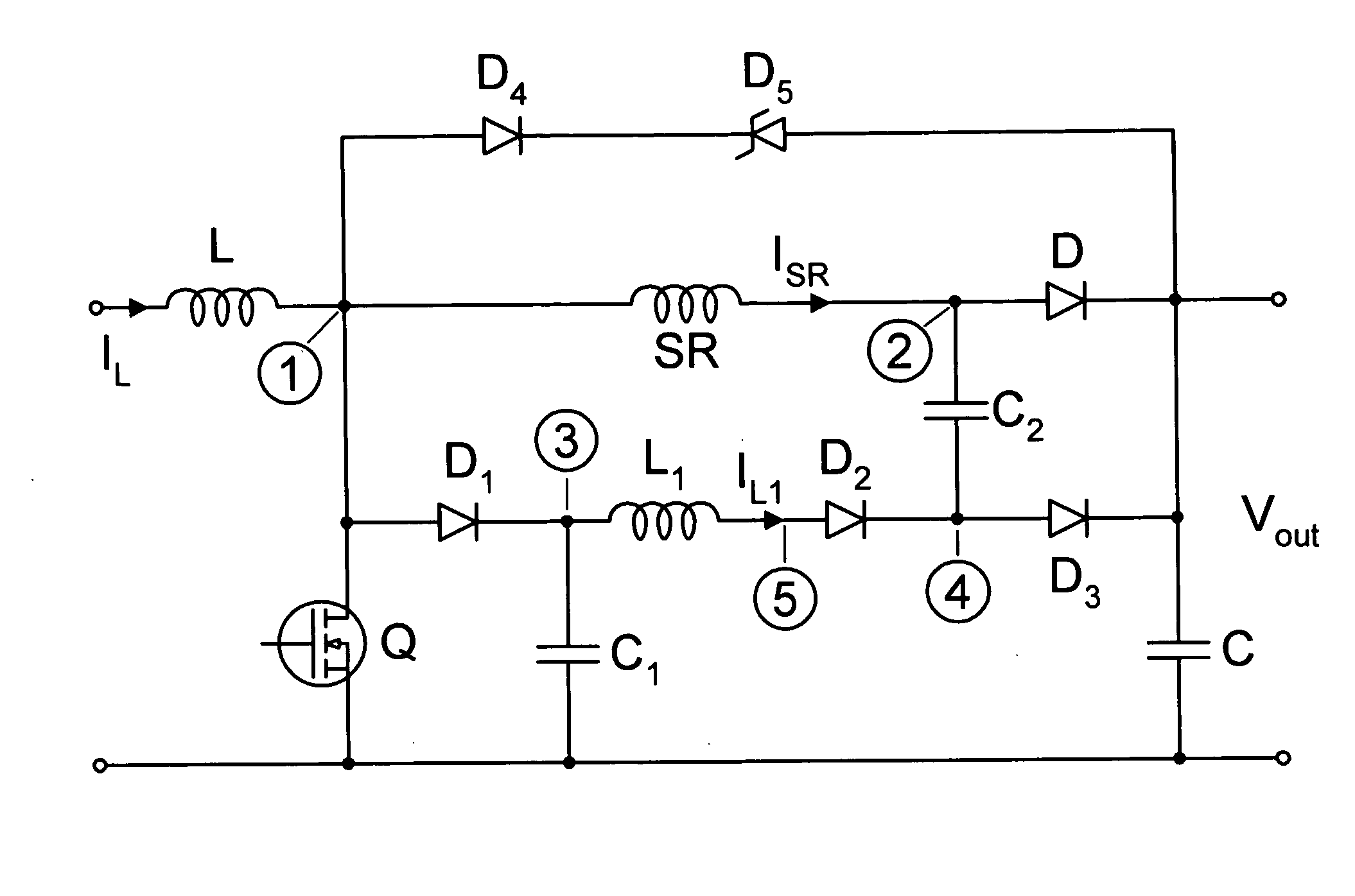
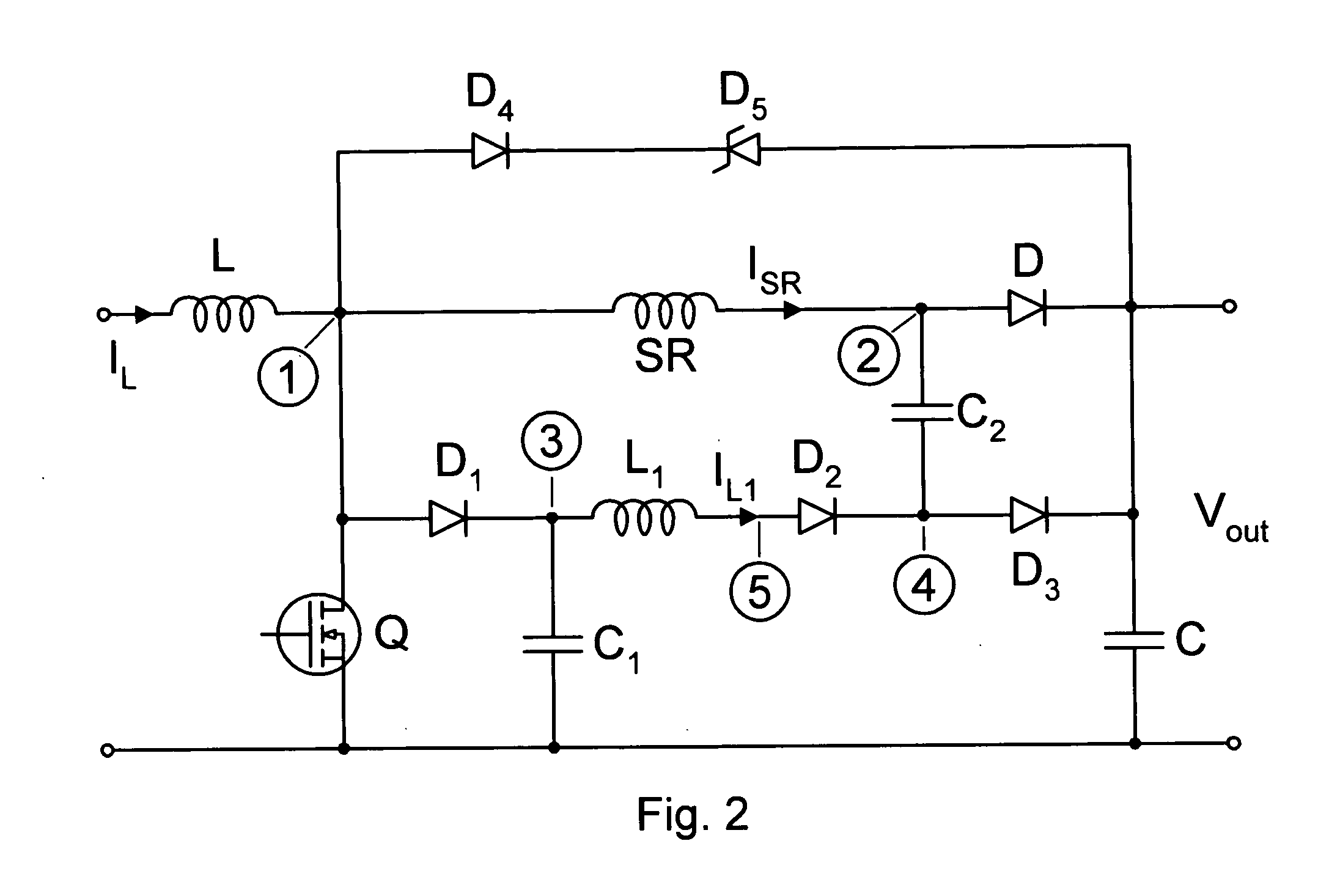
[0026] This is a functional description with idealized waveforms of the new non-dissipative snubber circuit during one switching cycle of the converter.

[0027] Interval (a)

[0028] During this interval (a), the main switch Q is turned-OFF so that input current IL flows trough the input inductor L, saturable reactor SR and the main diode D to the output capacitor C. The snubber circuit of the main switch Q is inactive during this interval (a) while capacitor C1 is charged to the output voltage Vout and capacitor C2 is discharged.

[0029] Interval (b)

[0030] This interval starts with the turn-ON of the main switch Q at which instant its voltage drops to zero almost immediately (waveform V1 for voltage of node 1 on FIG. 3a). Diode D1 prevents capacitor C1 from discharging through the turned-ON main switch Q, hence the voltage V3 of node 3 stays equal to the output voltage Vout (waveform V3 on FIG. 3a). When the main switch Q was turned-ON, the current IL which was flowing t...


PUM


Abstract

A new type of the passive non-dissipative snubber with a single saturable reactor improves the performance of the boost converter used as a front-end active Power Factor Correction (PFC) in two critical areas: excess voltage stresses caused by high voltage spikes on input high voltage switching transistor of the boost converter is eliminated and EMI noise is much reduced. The high voltage spike energy instead of being dissipated as in a dissipative snubber circuits is recovered resulting in increased conversion efficiency. High voltage spike elimination also allows use of lower voltage rated devices with lower ON resistance, hence further increasing the efficiency of the PFC boost converter.

Description

FIELD OF THE INVENTION [0001] This invention relates to the field of switching AC-to-DC and DC-to-DC power conversion and in particular to the new class of the non dissipative snubber circuit for the boost converter primarily (because of difficulties for soft switching implementation), but not limited only to it, which dramatically reduces the overvoltage stress on the MOSFET switch enabling use of the lower voltage rating components with lower RON resistance for the higher efficiency of the converter and at the same time significantly improves the EMI characteristics with implementation of the smaller, low-cost EMI filters. BACKGROUND OF THE INVENTION [0002] The IEC 1000-3-2 regulation demand that higher output power converters (currently over 75W) must have the front-end active Power Factor Correction (PFC) to meet the stringent requirements for the input current harmonics content. Thus, the front-end boost converter with active PFC feature is the most common solution present in t...

Claims


Application Information

Patent Timeline
Patent Type & Authority Applications(United States)
IPC IPC(8): H02H7/10
CPCH02M1/34Y02B70/1491H02M2001/346H02M3/155H02M1/346Y02B70/10
Inventor SCHENK, KURT
Owner TESLACO
Why Eureka
Try Eureka