Method of assembling electronic components of an electronic system, and system thus obtained

a technology of electronic systems and electronic components, applied in the field of electronic systems and systems, can solve the problems of affecting the performance of packaged components as little as possible, ptfe (polytetrafluoroethylene), and insufficient control of transmission line impedance values, etc., to achieve the effect of reducing the number of discontinuities

Inactive Publication Date: 2006-11-30
IBM CORP
View PDF3 Cites 15 Cited by
  • Summary
  • Abstract
  • Description
  • Claims
  • Application Information

AI Technical Summary

Benefits of technology

[0019] The Applicant has devised a new solution for assembling and, particularly, functionally connecting to each other components of an electronic system, that allows to substantially reduce t

Problems solved by technology

However, in applications involving high operating speeds, which are becoming more and more common, a further requirement of the packages is that they essentially maintain the performance levels of the electronic components they carry within, or that they affect the packaged components' performances as less as possible.
Controlling the transmission line impedance value is however not sufficient, due to the unavoidable presence of parasitic elements exhibiting a capacitive, resistive or inductive behavior, which parasitic elements are intrinsically embedded in the package, or in the PCBs, due to the association of materials and conductive structures needed to establish paths for electrical

Method used


Image

  • Method of assembling electronic components of an electronic system, and system thus obtained
  • Method of assembling electronic components of an electronic system, and system thus obtained
  • Method of assembling electronic components of an electronic system, and system thus obtained

Examples


Embodiment Construction

)

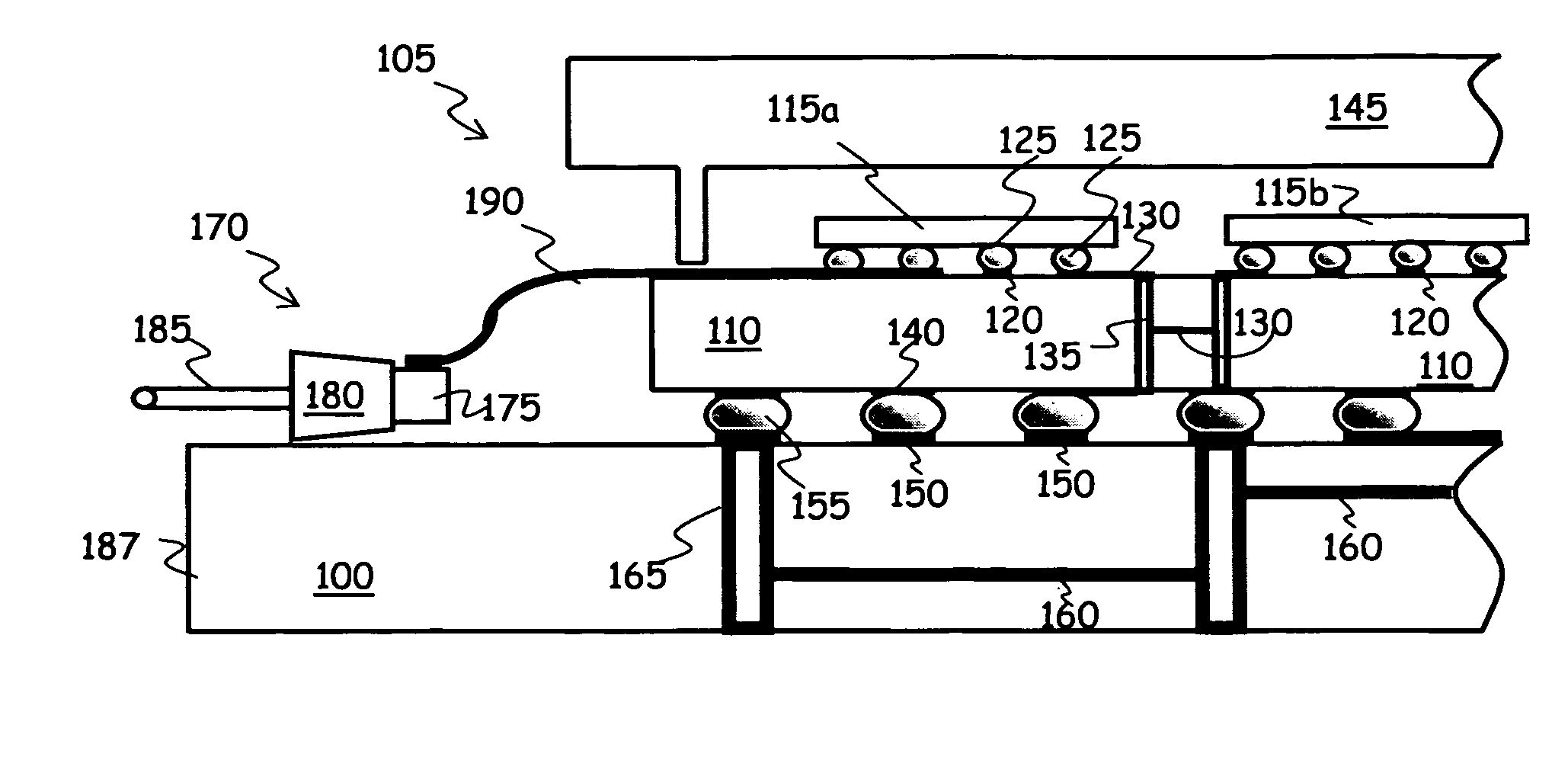
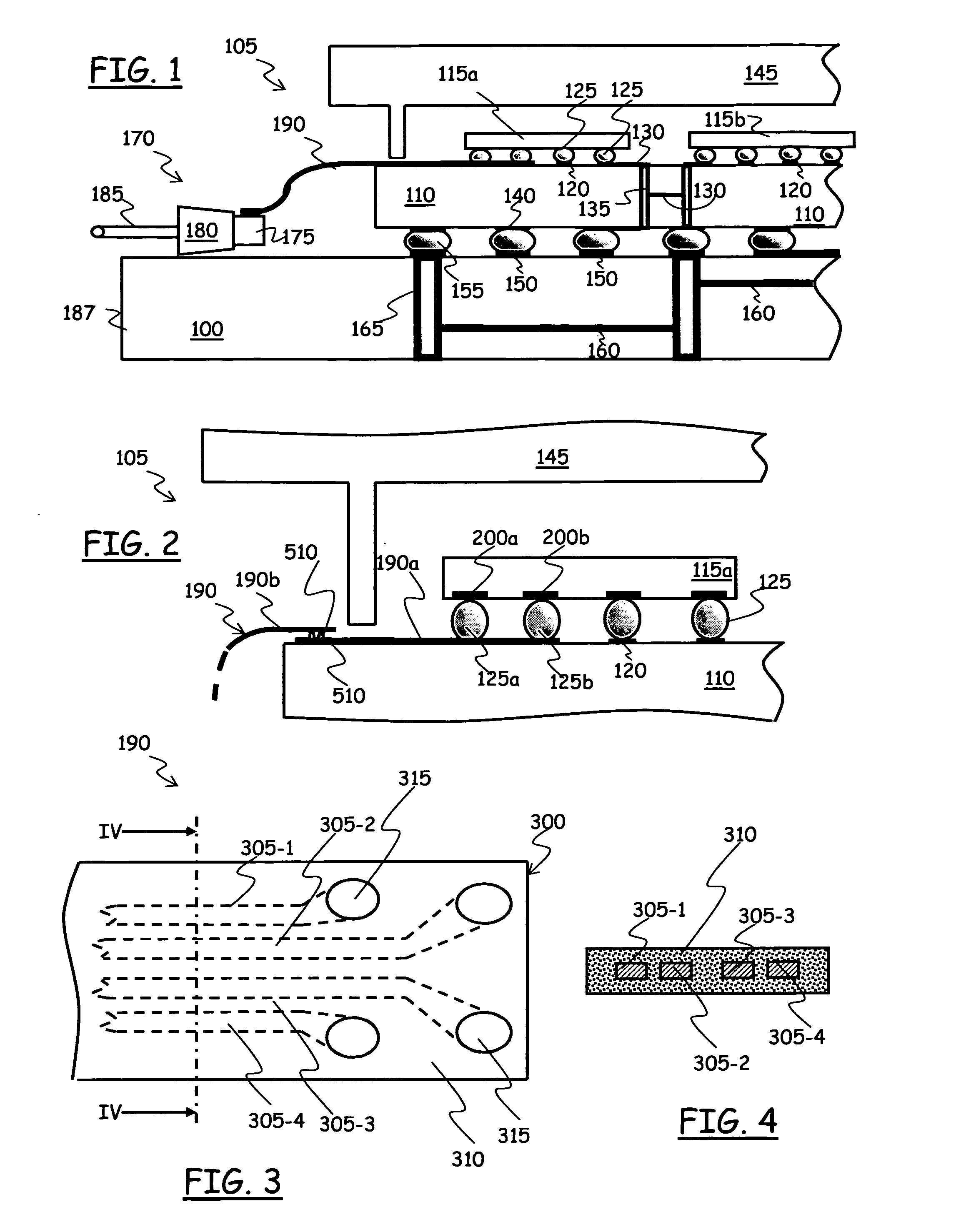
[0040] With reference to the drawings, in FIG. 1 there is shown, very schematically, a portion of a PCB 100 of an electronic system; for example, the electronic system may include several PCBs like the PCB 100, adapted to be connected to a backplane (not shown in the drawings) of a rack. The electronic system may for example be part of an optical communications system.

[0041] As visible in the drawing, an MCM package 105 is mounted to the PCB 100; schematically, the MCM package comprises an MCM substrate 110, made for example of a ceramic or organic (e.g., plastic) material. Two or more IC chips are mounted to the MCM substrate 110, like the two IC chips 115a and 115b shown in the drawing. The IC integrated in the chips mounted to the MCM substrate 110 can be of whatsoever type, their specific nature being not critical nor limitative to the present invention; in particular, the ICs can be standard or full-custom or ASIC chips, like for example a microprocessor IC (a CPU), a DSP IC,...


PUM

PropertyMeasurementUnit
Electrical conductivityaaaaaaaaaa
Flexibilityaaaaaaaaaa

Abstract

An electronic system comprising: an electronic system support substrate for the attachment of components of the electronic system, the electronic system support substrate including electric signal propagation paths for the propagation of electric signals between the system components; at least a first and a second electronic components wherein at least the first electronic component is part of a module in mechanical and electrical connection with the electronic system support substrate, the module comprising a module substrate to which the first electronic component is at least mechanically connected, and an electric coupling between the first and the second electronic components, for the electric coupling allowing the first and the second electronic components exchange of electric signals. The electric coupling comprises a direct electric connection particularly formed by a flexible electrical interconnection member, between the first and the second electronic components, the electric connection being independent of the electronic system support substrate.

Description

TECHNICAL FIELD [0001] The present invention relates to the field of electronic circuits and systems, particularly albeit not limitatively to systems including both electronic and optical components (hereinafter shortly referred to as opto-electronic systems). Specifically, the present invention relates to the aspects of packaging, assembling and functionally interconnecting the different systems' components. BACKGROUND ART [0002] Components of electronic or opto-electronic systems, such as for example Integrated Circuits (ICs) like data and / or signal processors (microprocessors, CPUs, DSPs, ASICs), photodetectors, semiconductor lasers, are usually packaged in respective packages, and then assembled to boards (Printed Circuit Boards—PCBs) that perform a double function of providing a mechanical support as well as a functional (electrical) interconnection between the different systems' components. [0003] One packaging solution known in the art, featuring a high packing efficiency, is...

Claims


Application Information

Patent Timeline
IPC IPC(8): H01L23/52
CPCH01L23/3121Y10T29/49144H01L23/49827H01L23/522H01L23/552H01L23/66H01L24/81H01L24/86H01L25/0655H01L25/167H01L2224/16H01L2224/48227H01L2224/49175H01L2224/81203H01L2224/81205H01L2224/81224H01L2224/81801H01L2924/01005H01L2924/01013H01L2924/01029H01L2924/01046H01L2924/01078H01L2924/01079H01L2924/01082H01L2924/09701H01L2924/14H01L2924/1433H01L2924/15173H01L2924/15311H01L2924/16152H01L2924/3011H01L2924/3025H05K1/141H05K1/147H05K1/189H05K3/222H05K3/3436H05K2201/045H05K2201/10121H05K2201/1053H05K2201/10674H01L23/49822H01L2224/16225H01L2224/73265H01L2924/014H01L2924/01047H01L2924/01033H01L24/48H01L24/49H01L2224/81143H01L2924/00H01L2924/12043H01L2924/181H01L2224/05553H01L2224/48091H01L2224/0401H01L2924/00014H01L2224/85207H01L2224/85205H01L2224/85203H01L2924/00012H01L2224/45099H01L2224/45015H01L2924/207
Inventor OFFREIN, BERT J.OGGIONI, STEFANO S.SPREAFICO, MAURO
Owner IBM CORP
Why Eureka
Try Eureka