Substrate for liquid crystal display device, liquid crystal display device having same, and driving method of liquid crystal display device

a technology of liquid crystal display device and substrate, which is applied in static indicating devices, instruments, non-linear optics, etc., can solve the problem of not providing superior display characteristics, and achieve the effect of superior display characteristics

Inactive Publication Date: 2006-11-30
SHARP KK
View PDF10 Cites 78 Cited by
  • Summary
  • Abstract
  • Description
  • Claims
  • Application Information

AI Technical Summary

Benefits of technology

[0021] An object of the present invention is therefore to provide a substrate for a liquid crystal display device capable of providing superior display characteristics, a liquid crystal display device having it, and a driving method of a liquid crystal display device.
[0023] The invention can realize a liquid crystal display device capable of providing superior display characteristics.

Problems solved by technology

As described above, conventional liquid crystal display devices that employ the capacitive coupling HT technique have a problem that they cannot provide superior display characteristics because of occurrence of the burn-in phenomenon though their viewing angle characteristic is good.

Method used


Image

  • Substrate for liquid crystal display device, liquid crystal display device having same, and driving method of liquid crystal display device
  • Substrate for liquid crystal display device, liquid crystal display device having same, and driving method of liquid crystal display device
  • Substrate for liquid crystal display device, liquid crystal display device having same, and driving method of liquid crystal display device

Examples


first embodiment

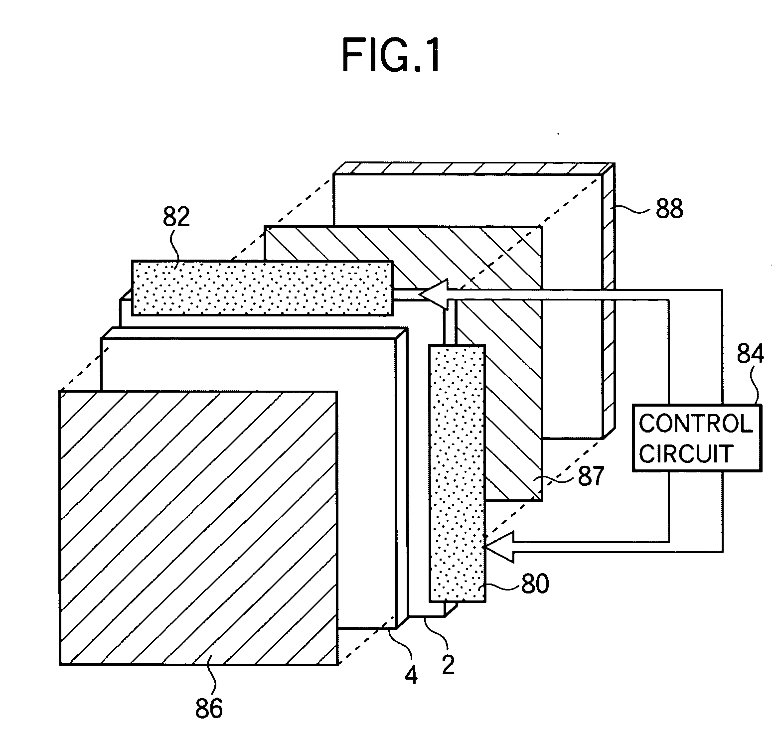
[0053] A substrate for a liquid crystal display device, a liquid crystal display device having it, and a driving method of a liquid crystal display device according to a first embodiment of the present invention will be hereinafter described with reference to FIGS. 1 to 12. FIG. 1 schematically shows the configuration of the liquid crystal display device according to the embodiment. As shown in FIG. 1, the liquid crystal display device has a TFT substrate 2 which is provided with gate bus lines and drain bus lines that cross each other with an insulating film interposed in between, TFTs that are formed for respective pixels, and pixel electrodes. The liquid crystal display device is also equipped with an opposite substrate 4 in which CFs and a common electrode are formed and a liquid crystal 6 (not shown in FIG. 1) that is sealed between the substrates 2 and 4 and has negative dielectric anisotropy, for example.

[0054] A gate bus line driving circuit 80 incorporating a driver IC for...

second embodiment

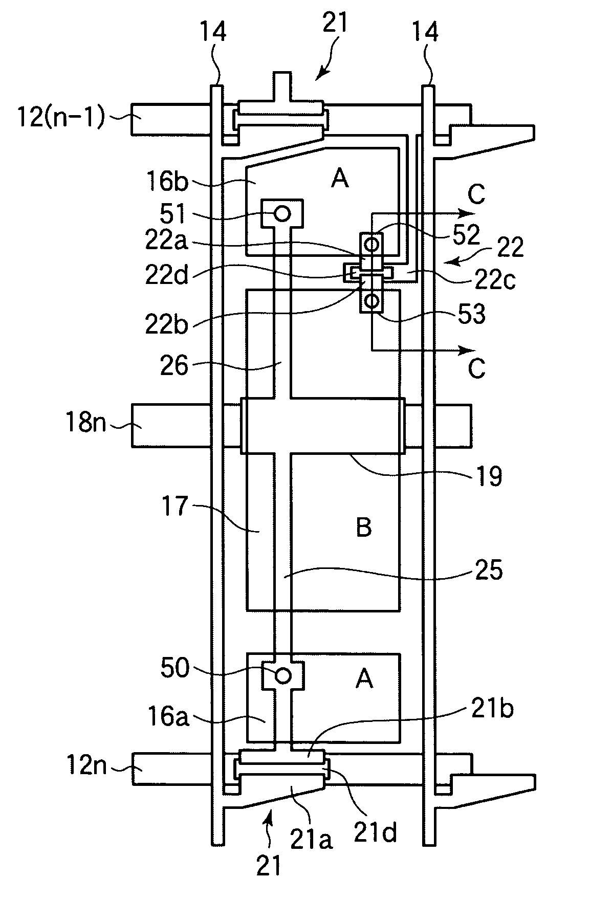
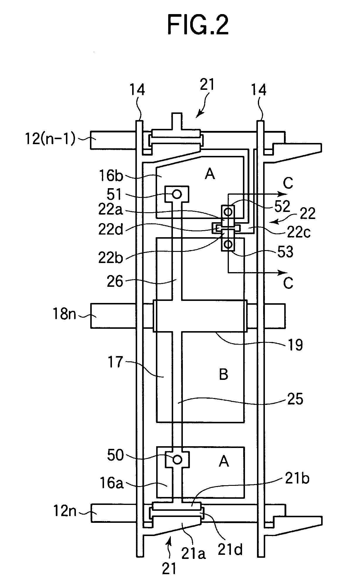
[0084] Next, a substrate for a liquid crystal display device, a liquid crystal display device having it, and a driving method of a liquid crystal display device according to a second embodiment of the invention will be hereinafter described with reference to FIGS. 13 to 21. FIG. 13 shows the configuration of one nth-row pixel of a substrate for a liquid crystal display device according to the embodiment. FIG. 14 shows an equivalent circuit of the one nth-row pixel of the liquid crystal display device according to the embodiment. As shown in FIGS. 13 and 14, this embodiment is characterized in that the storage capacitor bus line 18n is connected to the pixel electrode 17 of the sub-pixel B via a second TFT 22. A drain electrode (or source electrode) 22a of the TFT 22 is electrically connected to a link electrode 56 which is made of the same material and in the same layer as the pixel electrodes 16a, 16b, and 17 via a contact hole 55 which is formed through the protective film 32. The...

third embodiment

[0103] Next, a liquid crystal display device according to a third embodiment of the invention will be described with reference to FIG. 22. Whereas in the first and the second embodiments the pixel region is divided into two kinds of sub-pixels A and B, in this embodiment the pixel region is divided into three (or more) kinds of sub-pixels to further improve the viewing angle characteristic. FIG. 22 shows an equivalent circuit of one pixel of a liquid crystal display device according to this embodiment. As shown in FIG. 22, the liquid crystal display device according to this embodiment is different from that according to the first embodiment (see the equivalent circuit of FIG. 4) in that a second control capacitance Cc2 is provided in the same pixel as a first control capacitance Cc1 (in FIG. 4, the control capacitance Cc) is provided. One electrode of the second control capacitance Cc2 is electrically connected to the source electrode of the TFT 21. The other electrode of the second...


PUM

PropertyMeasurementUnit
polar angleaaaaaaaaaa
timeaaaaaaaaaa

Abstract

The invention relates to a substrate for a liquid crystal display device, a liquid crystal display device having the substrate, and a driving method of a liquid crystal display device and provide a substrate for a liquid crystal display device capable of providing superior display characteristics, a liquid crystal display device having it, and a driving method of a liquid crystal display device. A substrate for a liquid crystal display device is provided with a pixel region having first sub-pixels in which respective first pixel electrodes are formed and a second sub-pixel in which a second pixel electrode is formed, a first TFT having a gate electrode that is connected to an nth gate bus line and a source electrode that is connected the first pixel electrodes, a second TFT having a gate electrode that is connected to an (n−1)th gate bus line, a drain electrode that is connected to the source electrode of the first TFT, and a source electrode that is connected to the second pixel electrode, and a control capacitance section which establishes capacitive coupling between the source electrode of the first TFT and the second pixel electrode.

Description

BACKGROUND OF THE INVENTION [0001] 1. Field of the Invention [0002] The present invention relates to a substrate for a liquid crystal display device used as, for example, a display unit of an electronic apparatus, a liquid crystal display device having the substrate, and a driving method of a liquid crystal display device. [0003] 2. Description of the Related Art [0004] In recent years, liquid crystal display devices have come to be used for TV receivers, monitor devices of personal computers, etc. In these purposes, liquid crystal display devices are required to have a good viewing angle characteristic that the display screen is viewable from all directions. FIG. 23 is a graph showing transmittance vs. application voltage characteristics (T-V characteristics) of a VA (vertically aligned)-mode liquid crystal display device. The horizontal axis represents the voltage (V) applied to the liquid crystal layer and the vertical axis represents the light transmittance. Line A is a T-V char...

Claims


Application Information

Patent Timeline
Patent Type & Authority Applications(United States)
IPC IPC(8): G02F1/1343
CPCG02F1/134309G02F1/136213G02F2001/134345G02F2201/123G09G2320/028G09G2300/0443G09G2300/0809G09G2320/0257G09G3/3659G02F1/134345G02F1/133
Inventor KAMADA, TSUYOSHINAKANISHI, YOHEIUEDA, KAZUYAYOSHIDA, HIDEFUMITSUDA, HIDEAKI
Owner SHARP KK
Why Eureka
Try Eureka