Display device, and computer, camera, portable information terminal device, image reproducing device, clock, mobile phone device and other electronic apparatuses using the display device

Inactive Publication Date: 2006-12-07
SEMICON ENERGY LAB CO LTD
View PDF37 Cites 44 Cited by
  • Summary
  • Abstract
  • Description
  • Claims
  • Application Information

AI Technical Summary

Benefits of technology

[0020] As described above, according to the invention, a shape of a pixel electrode is formed to be an octagon, thereby arrangement of elements is performed effectively while performing a delta arrangement, so that parasitic resistanc

Problems solved by technology

There is a defect as described below in the aforementioned conventional display device.
However, since pixels are arranged while shifting by one-half every other column, a wire for supplying a signal and a wire for supplying power source to elements of a pixel becomes complicated so that much area is required between pixel electrodes, and parasitic resistance and parasitic capacitance of the wires are increased.
Particularly, in a case

Method used


Image

  • Display device, and computer, camera, portable information terminal device, image reproducing device, clock, mobile phone device and other electronic apparatuses using the display device
  • Display device, and computer, camera, portable information terminal device, image reproducing device, clock, mobile phone device and other electronic apparatuses using the display device
  • Display device, and computer, camera, portable information terminal device, image reproducing device, clock, mobile phone device and other electronic apparatuses using the display device

Examples


embodiment 1

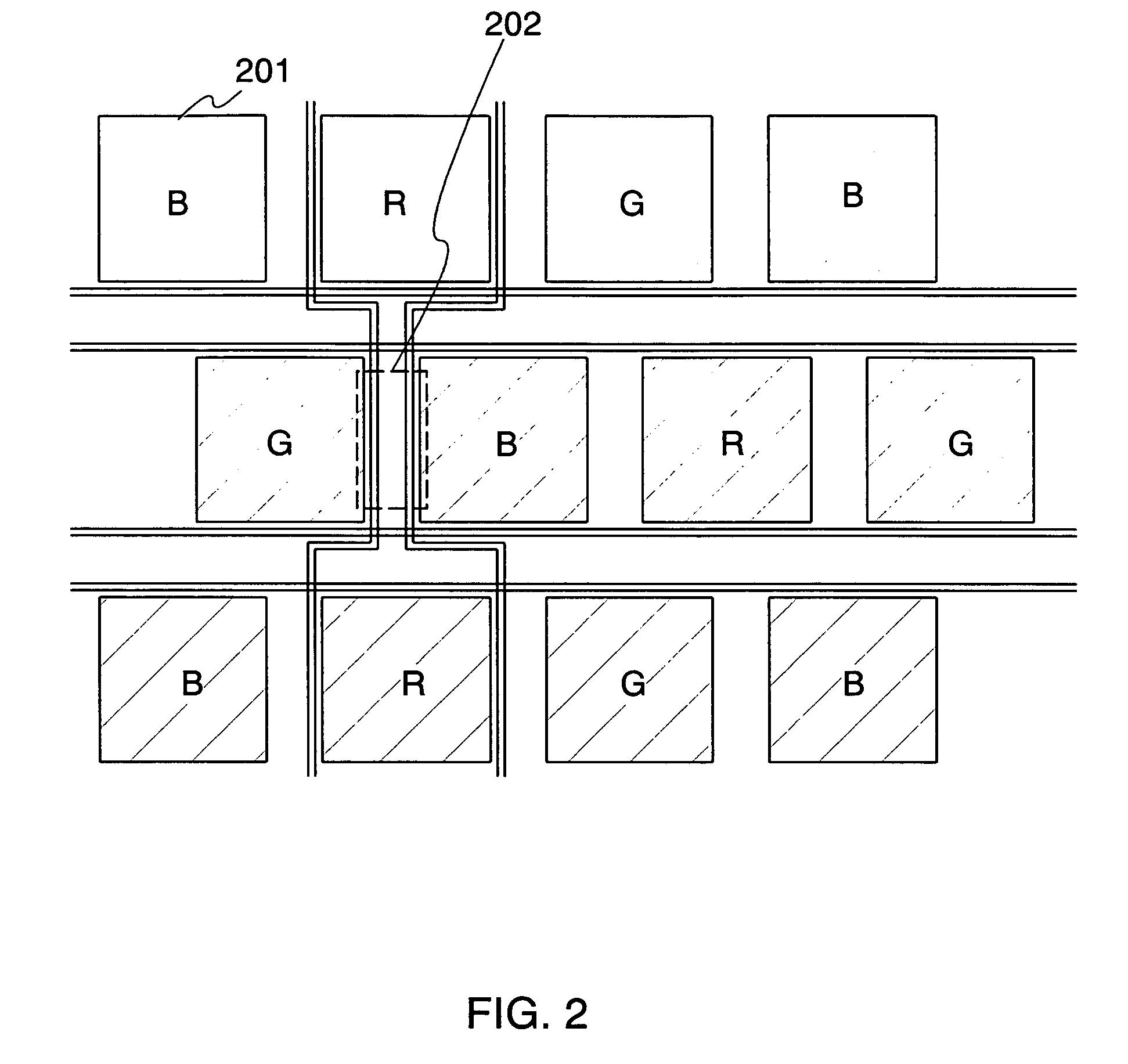
[0040]FIG. 4 shows an example of a circuit configuration of 301 shown in FIG. 3. Reference numeral 401 of FIG. 4 corresponds to the circuit 311 of FIG. 3. In FIG. 4, reference numeral 402 denotes a data line, 421 denotes a first scan line, 404 denotes a second scan line, 403 denotes a power supply line, 405 denotes a switch TFT, 409 denotes a driving TFT, 415 denotes a light-emitting element, 417 denotes a first electrode of the light-emitting element, and 416 denotes a second electrode of the light-emitting element. In addition, TFTs 410 to 413 form a static memory. Reference numeral 406 denotes a switch TFT for easily writing to the static memory and uses a TFT with reverse polarity to the switch TFT 405. In addition, 407 denotes a switch TFT for inputting an output of the static memory into a gate of the driving TFT 409. A switch TFT 408 is for connecting the gate of the driving TFT 409 to the power supply line 403, and is used to turn off the driving TFT 409. Reference numeral 4...

embodiment 2

[0045] Since an output value of a static memory is a digital value to express 0 or 1, display using the static memory cannot be performed in an analog manner. Therefore, when a gray scale display is performed, a time gray scale method is used. A principle of the time gray scale method is described.

[0046] In a case of a time gray scale method, gradation is expressed by changing light emitting time of an element which emits light with a certain constant luminance. For example, when light emits during one frame period entirely, lighting ratio becomes 100%. In addition, when light emits during half period of one frame period, lighting ratio becomes 50%. When the frame frequency is high to some extent, in a case of 60 Hz or more in general, human eyes cannot recognize blinking but recognize a halftone. In this manner, lighting ratio is changed so that the gradation can be expressed.

[0047] In FIG. 5A, an abscissa indicates time and an ordinate indicates pixels arranged in a row directio...

embodiment 3

[0057] Description is made on a circuit for supplying a signal for performing a time gray scale driving method to a source driver circuit and a gate driver circuit of a display with reference to FIGS. 7 and 8.

[0058] In this specification, a video signal inputted to a display device is called a digital video signal. Note that here, description is made on a display device in which a digital video signal of 4 bits is inputted to display an image as an example. However, the invention is not limited to 4 bits.

[0059] A digital video signal is read to a signal control circuit 701 and a digital video signal (VD) is outputted to a display 700. In addition, in this specification, a digital video signal which is edited in the signal control circuit to be converted to a signal to be inputted in the display is called the digital video signal. Signals for driving a source driver circuit 707 and a gate driver circuit 708 in the display 700 are inputted by a display controller 702.

[0060] Descrip...


PUM


Abstract

In a display device using a delta arrangement, in a case where a circuit of a large number of elements such as a static memory is arranged every pixel, a wire becomes complicated to cause wiring delay. A shape of a pixel electrode is formed polygonally to arrange in a case where the number of elements such as a static memory is large or in a case where an area of an element required to be included in a pixel is large in a delta arrangement. The shape of the pixel electrode is arranged in a polygon so that a wire along a pixel shape can be used. Even in a case of a pixel with a large number of elements, parasitic resistance of a wire and parasitic capacitance of a wire can be reduced so that wiring delay can be solved.

Description

BACKGROUND OF THE INVENTION [0001] 1. Field of the Invention [0002] The present invention relates to a display device, and particularly relates to a display device having a light-emitting element. In addition, the invention relates to an electronic apparatus including the display device having a light-emitting element. [0003] 2. Description of the Related Art [0004] In recent years, a mobile phone is widespread with the advance of communication technology. It is expected that a moving image will be transferred further and more amount of information will be transmitted in the future. On the other hand, a personal computer (PC) for mobile use has been produced due to the weight reduction. An information terminal called a PDA originated in an electronic notebook is produced a lot and being widespread. In addition, with development of display devices, the majority of such portable information devices is provided with a flat panel display. [0005] Moreover, in recent years, in an active m...

Claims


Application Information

Patent Timeline
IPC IPC(8): G09G5/02H05B44/00
CPCG09G3/2022G09G3/2025G09G3/2037G09G3/2092G09G3/3258G09G5/399G09G2360/18G09G2300/0443G09G2300/0857G09G2340/0414G09G2340/0421G09G2340/145G09G2360/02G09G2300/0417
Inventor KOYAMA, JUNMIYAKE, HIROYUKIYAMAZAKI, SHUNPEI
Owner SEMICON ENERGY LAB CO LTD
Why Eureka
Try Eureka