Supercharge Your Innovation With Domain-Expert AI Agents!

Conductive spacers for liquid crystal displays

a technology of liquid crystal display and spacer, which is applied in the direction of instruments, non-linear optics, optics, etc., can solve the problems of lcd (the pixels) malfunction, module or related parts with a larger size, and burnout of ito circuit, so as to reduce unwanted voltage and promote the ability of the modified lcd to withstand static charg

Inactive Publication Date: 2006-12-07
WINTEK CORP
View PDF9 Cites 5 Cited by
  • Summary
  • Abstract
  • Description
  • Claims
  • Application Information

AI Technical Summary

Benefits of technology

[0009] To solve the aforesaid disadvantages, the primary object of the present invention is to make spacers conductive in the liquid crystal layer of a LCD in which the spacers originally provides a function of anchoring the upper and lower board and now also forms a conductive path to reduce the unwanted voltage built between the upper and lower sides of the liquid crystal layer. The capability of the modified LCD to withstand the static charge will be promoted.
[0010] Since the slightly leaky liquid crystals and the conductive spacers provide two equivalent resistors in parallel with each other, another object of the invention is to decrease the partial voltage exerted on the liquid crystal layer from the external high-voltage static charges by the smaller resistance formed by the liquid crystals and the spacers. The damage in the liquid crystal layer from the external static charge source is thereby reduced. The display quality and its reliability of the LCD panel can also be pertained.
[0012] By means of the above construction set forth, the liquid crystals and the spacers in the liquid crystal layer play as two resistors that are coupled in parallel. The partial voltage found in the liquid crystal layer will be smaller so that the damaging effect of the external electrostatic charge source on the liquid crystals in the liquid crystal layer will be reduced. Therefore the display quality of the display panel may be pertained as desired and the capability of the LCD to withstand the electrostatic charge is enhanced.

Problems solved by technology

For conventional LCD products exposed in an environment of high-voltage electrostatic charges, instantaneous injection of the charges would either cause burnout of the ITO circuits or make the LC cells (the pixels) malfunctioning.
However, this approach usually results in the penalty of larger size for the modules or related parts, and hence a higher cost for products.
Since the LC molecules are affected by the electric field, the display quality will be deteriorated if there are trapped charges in the LC cells.
This is still a serious issue not totally solved by conventional discharging approaches.
Both will result in a much higher cost in fabrication.
These special lines will make the design of the interconnection layout more complicated.
Even with a conductive layer coated on the entire outer surface of the board will also increase the fabrication cost.
This makes the structure more complicated, and also increases the manufacturing cost.

Method used


Image

  • Conductive spacers for liquid crystal displays
  • Conductive spacers for liquid crystal displays
  • Conductive spacers for liquid crystal displays

Examples


Embodiment Construction

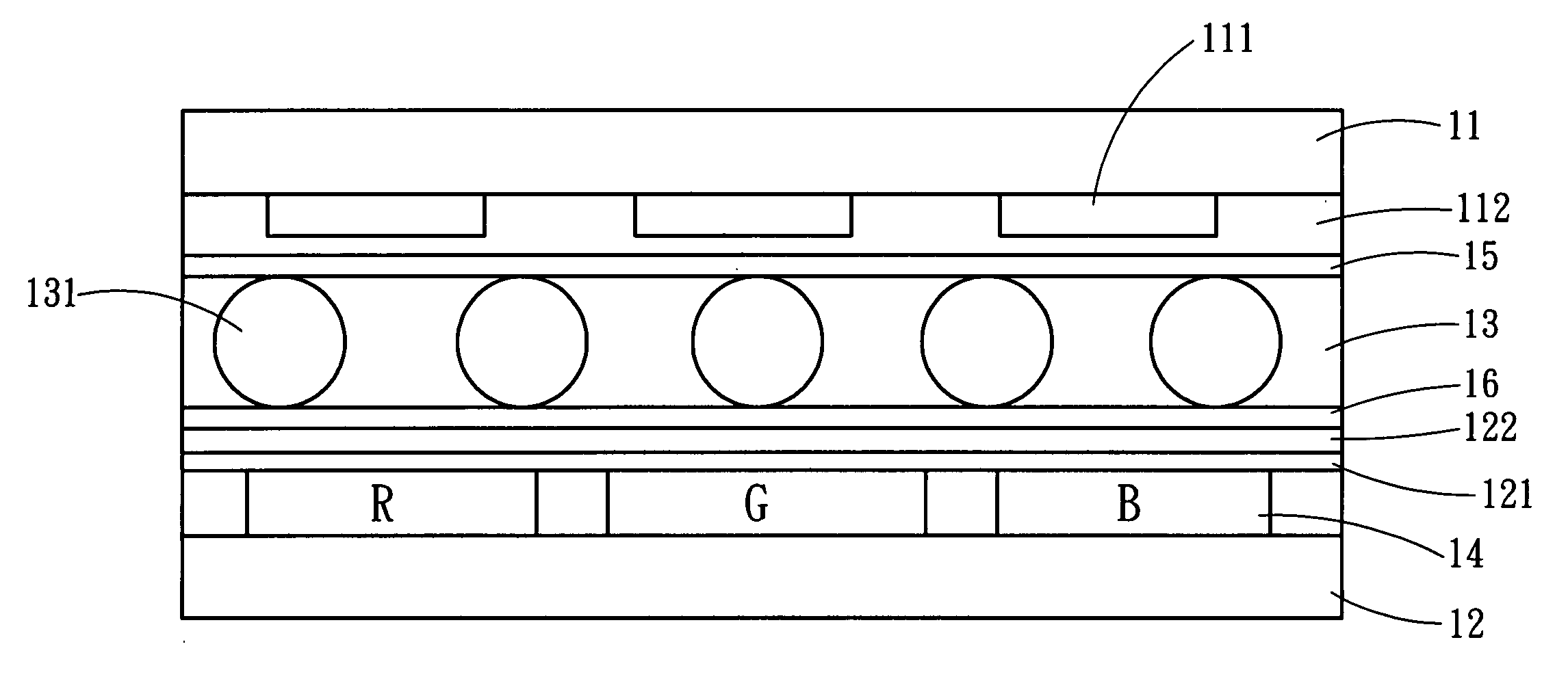
[0017] Please refer to FIG. 1, the fundamental manufacturing process of the LCD according to the invention is substantially same as that of the conventional LCD. The LCD of the invention includes an upper board 11 and a lower board 12 that couple to each other with a space interposed between them. The surfaces of the upper board 11 and the lower board 12 that face to each other have respectively transparent electrode layers 111 and 121 formed with a patterned pixel circuit, and insulation layers 112 and 122 covering the transparent electrode layers 111 and 121. On the surface of the transparent electrode layer 121 of the lower board 12, there is a color filter 14. On the surfaces of the insulation layers 112 and 122 that face to each other, there are respectively polyimides 15 and 16.

[0018] There is a liquid crystal layer 13 sandwiched between the upper board 11 and the lower board 12 and a plurality of spacers 131 located in the space between the upper board 11 and the lower board...


PUM

PropertyMeasurementUnit
transparentaaaaaaaaaa
conductiveaaaaaaaaaa
electrically conductiveaaaaaaaaaa

Abstract

A liquid crystal display (LCD) includes an upper board and a lower board that couple each other and form a space therebetween, a liquid crystal layer sandwiched between the upper board and the lower board and a plurality of spacers located in the space between the upper board and the lower board. The spacers are conductive so that the liquid crystal layer and the spacers form two equivalent parallel resistive paths to conduct the extra charges in the liquid crystals. When the LCD is subject to an external high static charge source, the static partial voltage found in the liquid crystal layer is reduced because of the lower equivalent parallel resistance, thus the damage and the interference on the liquid crystals in the liquid crystal layer caused by the external static charge source may be reduced.

Description

FIELD OF THE INVENTION [0001] The present invention relates to a technique to reduce the partial voltage exerted from an external static charge source on the liquid crystal layer in liquid crystal displays (LCDs) to mitigate the damaging effect of the charges on the liquid crystals (LCs) such that the capability of the LCD to withstand high-voltage electrostatic charges will be enhanced. BACKGROUND OF THE INVENTION [0002] For conventional LCD products exposed in an environment of high-voltage electrostatic charges, instantaneous injection of the charges would either cause burnout of the ITO circuits or make the LC cells (the pixels) malfunctioning. A guarding element or structure against electrostatic discharging (ESD) is necessary and usually found in designing the entire module. However, this approach usually results in the penalty of larger size for the modules or related parts, and hence a higher cost for products. [0003] Several approaches have been proposed to diminish the dam...

Claims


Application Information

Patent Timeline
Patent Type & Authority Applications(United States)
IPC IPC(8): G02F1/1339
CPCG02F2202/022G02F1/1339
Inventor LIU, TANG-CHIEHLIANG, BAU-JYWU, MING-KUNGHSIAO, YI-FANLI, YA-WEN
Owner WINTEK CORP
Features
  • R&D
  • Intellectual Property
  • Life Sciences
  • Materials
  • Tech Scout
  • Unparalleled Data Quality
  • Higher Quality Content
  • 60% Fewer Hallucinations
Learn More