Electrophoretic display apparatus and driving method thereof
a display apparatus and electrophoretic technology, applied in the field of display apparatus, can solve the problems of reducing the life of the display apparatus and a contrast, unable to obtain predetermined gradation optical level, and consequently applying dc voltage to the display device for a long time, so as to prevent the accumulation of residual dc components
- Summary
- Abstract
- Description
- Claims
- Application Information
AI Technical Summary
Benefits of technology
Problems solved by technology
Method used
Image
Examples
example 1
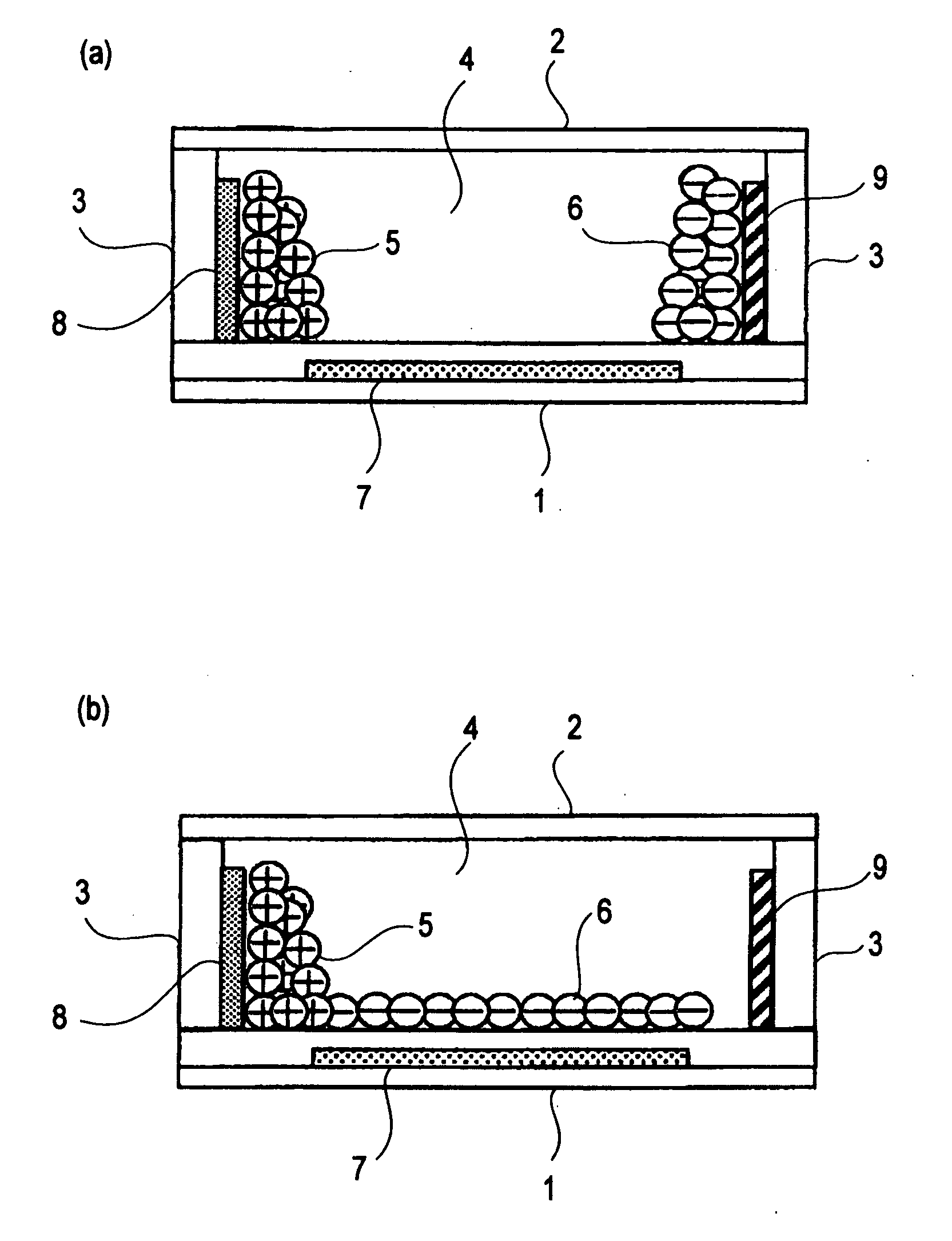
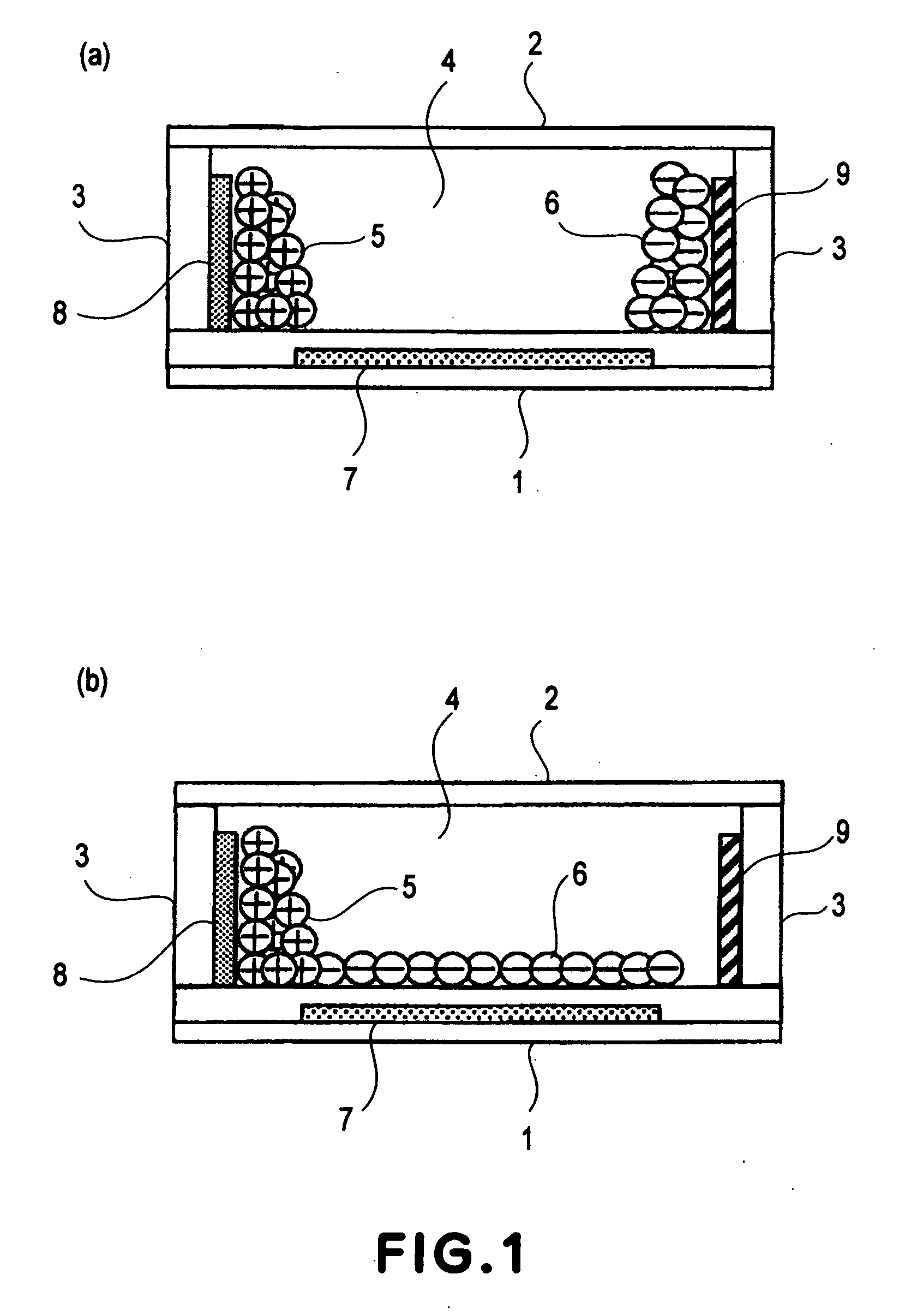
[0110] In this example, an electrophoretic display apparatus including the electrophoretic display device shown in FIGS. 1(a) and 1(b) according to First Embodiment of the present invention is prepared in the following manner. The electrophoretic display device includes a matrix panel having 600×1800 pixels. Further, each of the pixels has a rectangular planar shape as shown in FIG. 7 and has a size of 40 μm (width)×120 μ (length).
[0111] On a 1.1 mm-thick glass substrate as a first substrate 1, a thin film transistor (TFT) (not shown) and an IC (not shown), and other wirings necessary for drive are formed and thereon, an Si3N4 film as an insulating film is formed at the entire surface of the first substrate 1. Then, an Al layer is formed and subjected to patterning to form a first electrode 7. Incidentally, the first electrode 7 is communicated with the TFT through a contact hole which has been formed in advance.
[0112] Next, after the first electrode 7 is formed, a white (coloring...
example 2
[0127] In this example, an electrophoretic display apparatus including the electrophoretic display device shown in FIGS. 5(a) and 5(b) is prepared in the following manner. The electrophoretic display device includes a matrix panel having 600×1800 pixels. Further, each of the pixels has a rectangular planar shape as shown in FIG. 9 and has a size of 40 μm (width)×120 μ (length). In this example, electrodes include a first electrode 71 and a second electrode 81 as described above.
[0128] On a 1.1 mm-thick glass substrate as a first substrate 1, a thin film transistor (TFT) (not shown) and an IC (not shown), and other wirings necessary for drive are formed and thereon, an Si3N4 film as an insulating film is formed at the entire surface of the first substrate 1. Then, an Al layer is formed and subjected to patterning to form a first electrode 71. Incidentally, the first electrode 71 is communicated with the TFT through a contact hole which has been formed in advance.
[0129] Further, a s...
example 3
[0147] In this example, an electrophoretic display apparatus is prepared and subjected to the display operations in the same manner as in Example 2.
[0148] A driving method of the tested matrix panel will be described with reference to FIGS. 11(a) and 11(b).
[0149] Also in this example, display rewriting is performed in such a manner that the display operation shown in FIG. 10(a) and the display operation shown in FIG. 10(b) are alternatively repeated. More specifically, in this example, every two adjacent pixels, the first display operation and the second display operation are repetitively performed alternately while performing the reset operation between the display operations shown in FIGS. 8(a) and 8(b). In this driving method, a polarity of voltage applied is changed for each adjacent pixel. Accordingly, this driving method is referred to as a “dot inversion driving method”.
[0150] The electrophoretic display apparatus in this example has a memory characteristic with respect to...
PUM
 Abstract
Description
Claims
Application Information


