Imaging device and digital camera

a technology which is applied in the field of imaging device and digital camera, can solve the problems of inability to adjust the curvature of the microlenses, fail to perform an acceptable light condensing operation, and the microlenses do not always have the desired shape or index distribution, etc., and achieve the effect of improving the sensitivity of the image sensor chip and the quantum efficiency of the photodiod

Inactive Publication Date: 2006-12-14
FUJIFILM CORP
View PDF7 Cites 184 Cited by
  • Summary
  • Abstract
  • Description
  • Claims
  • Application Information

AI Technical Summary

Benefits of technology

[0014] According to the present invention, it is possible to adjust the air pressure inside the package that contains the image sensor chip. Since the microlenses made of a gel-like material transform in response to the change of the air pressure inside the package, the curvature of the microlenses can be changed according to the characteristics of a...

Problems solved by technology

Accordingly, the microlenses do not always have a desired shape or index distribution, and sometimes fail to perform an acceptable light condensing operation.
It is ther...

Method used


Image

  • Imaging device and digital camera
  • Imaging device and digital camera
  • Imaging device and digital camera

Examples


Embodiment Construction

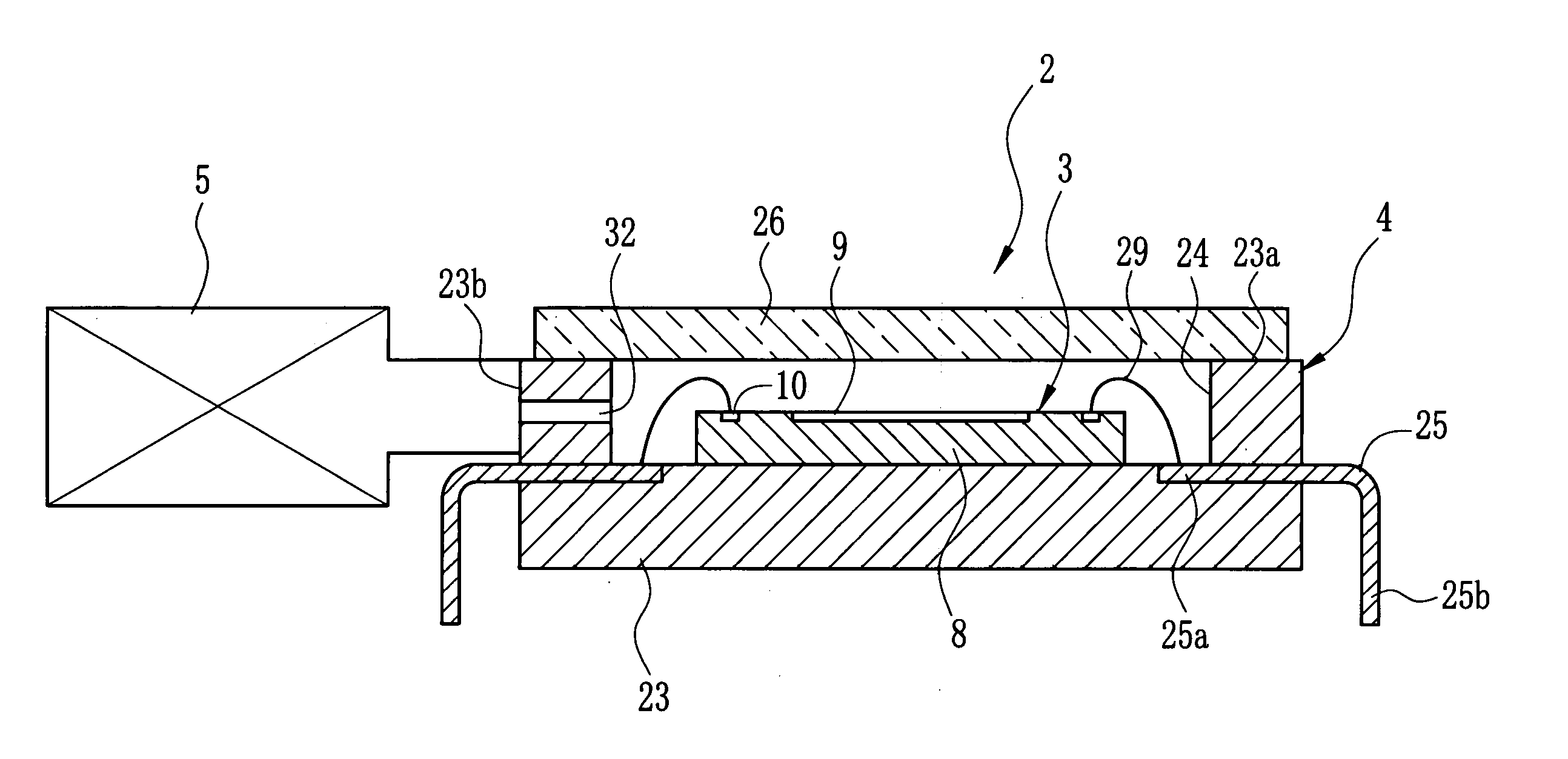
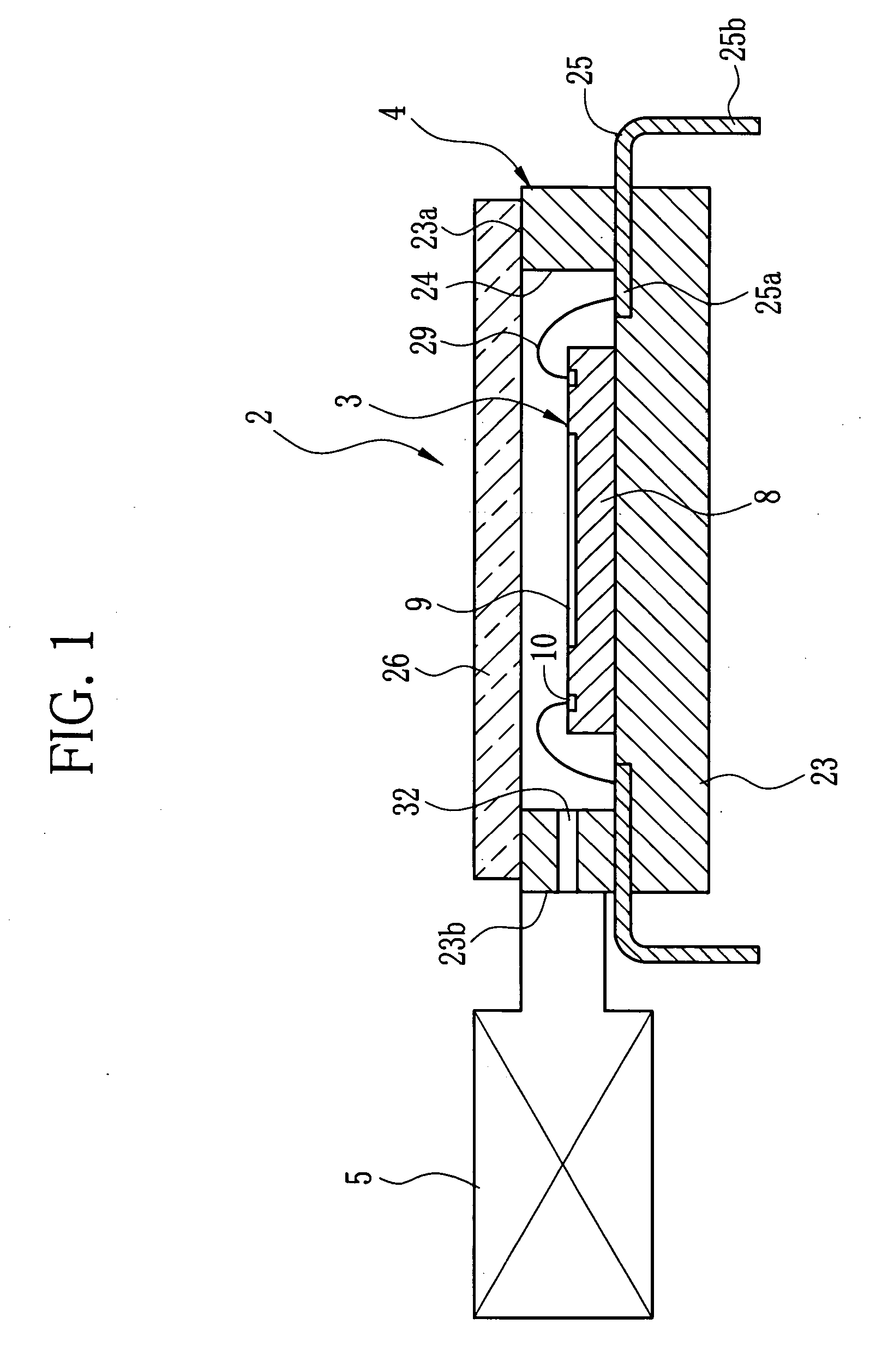
[0019] As shown in FIG. 1, an imaging device 2 of the present invention includes an image sensor chip 3, and a package 4 for containing the image sensor chip 3, and an air pump 5 connected to the package 4.

[0020] The image sensor chip 3 is composed of a chip substrate 8 of silicon or the like, whose top surface is provided with a light receiving area 9 and plural input / output pads 10. In the light receiving area 9, a plurality of photodiodes that perform a photoelectric conversion are arranged in a matrix from. The input / output pads 10 are electrode pads made of a conductive metal material, and electrically connected to the light receiving area 9.

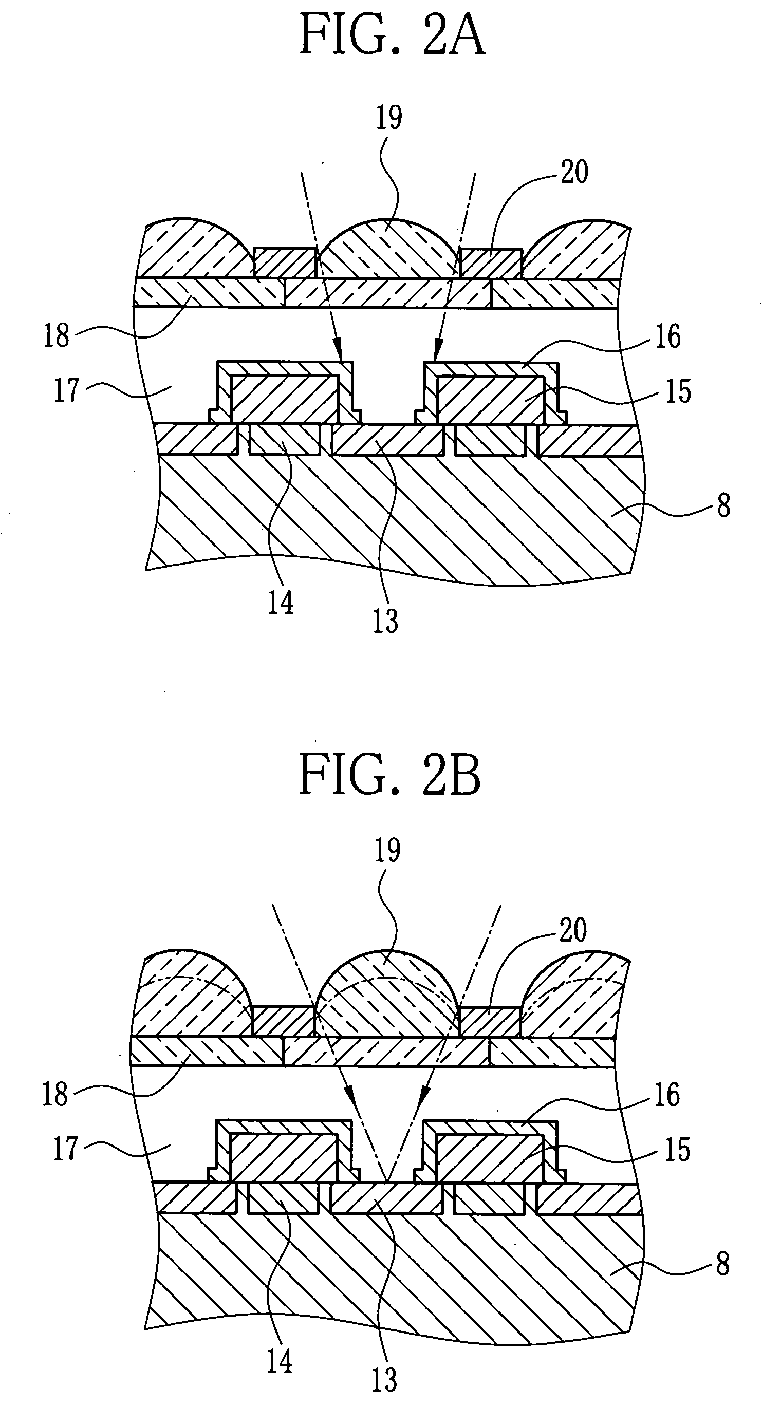
[0021] As shown enlarged in FIG. 2A, the light receiving area 9 on the top surface of the chip substrate 8 has photodiodes 13, and a plurality of vertical transfer CCDs 14 for transferring signal charges accumulated in the photodiodes 13. Disposed on the photodiode 13 and the adjoining vertical transfer CCD 14 is an electrode gate 15 whic...


PUM


Abstract

An imaging device includes an image sensor chip and a package for containing the image sensor chip. Formed in the package is a vent hole that is connected to an air pump. In a light receiving area of the image sensor chip, there are photodiodes and microlenses above them. The microlenses are made of a gel-like transparent material. When the internal air pressure of the package is changed by the air pump, each microlens transforms in response to the change of the internal air pressure, and thereby changes the surface curvature thereof.

Description

BACKGROUND OF THE INVENTION [0001] 1. Field of the Invention [0002] The present invention relates to imaging devices and digital cameras, and more particularly to an imaging device and a digital camera which use an image sensor chip having microlenses on photodiodes. [0003] 2. Description Related to the Prior Art [0004] Typical conventional imaging devices use a box-like package to contain an image sensor chip such as CCD image sensor or CMOS image sensor. Inside the package, the image sensor chip is connected to leads of the package through bonding wires, and the package is sealed with a transparent plate called a cover. The image sensor chip, for example, the CCD image sensor is made of a chip substrate whose top surface accommodates various component, such as a plurality of photodiodes that constitute a light receiving area, gate electrodes for reading out electric charges from the photodiodes, vertical transfer CCDs and a horizontal transfer CCD for transferring the electric cha...

Claims


Application Information

Patent Timeline
IPC IPC(8): H04N5/335H04N101/00
CPCG02B3/0018G02B3/14H01L27/14618H04N5/232H01L27/14627H04N5/2251H04N5/2253H01L27/14621H01L2224/48091H01L2224/48247H04N23/54H04N23/55H01L2924/00014
Inventor SENBA, TAKEHIKOMISAWA, TAKESHI
Owner FUJIFILM CORP
Why Eureka
Try Eureka