Quantum dots, methods of manufacturing quantum dots and methods of manufacturing organic light emitting display devices using the same

a technology of light emitting display device and quantum dots, which is applied in the direction of solid-state devices, chemistry apparatuses and processes, and light sources. it can solve the problems of poor current efficiency, low luminance, and poor quantum efficiency of quantum dots, and achieve high quantum efficiency, high quantum efficiency, and easy to obtain

Active Publication Date: 2017-05-11
SAMSUNG DISPLAY CO LTD +1
View PDF2 Cites 2 Cited by
  • Summary
  • Abstract
  • Description
  • Claims
  • Application Information

AI Technical Summary

Benefits of technology

This patent is about a method to make organic light emitting display devices that have high brightness and efficiency using quantum dots. The method involves controlling the reaction of a ligand and a shell forming precursor to form a strong chemical bond. An additional shell can be added to protect the quantum dot and ensure high quantum efficiency. The quantum dot can be used in the OLED device and results in high luminance and current efficiency with low current density. The quantum efficiency of the blue quantum dot is similar or better than that of green or red quantum dots.

Problems solved by technology

Therefore, the quantum dot may have poor quantum efficiency, and also an organic light emitting display (OLED) device including an emitting layer formed using (utilizing) the quantum dot may have low luminance and poor current efficiency.

Method used


Image

  • Quantum dots, methods of manufacturing quantum dots and methods of manufacturing organic light emitting display devices using the same
  • Quantum dots, methods of manufacturing quantum dots and methods of manufacturing organic light emitting display devices using the same
  • Quantum dots, methods of manufacturing quantum dots and methods of manufacturing organic light emitting display devices using the same

Examples


example 1

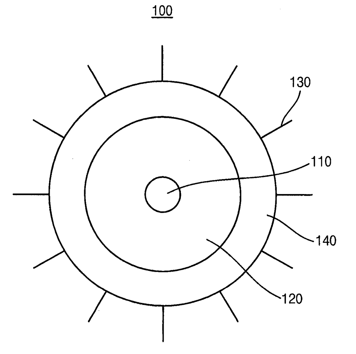
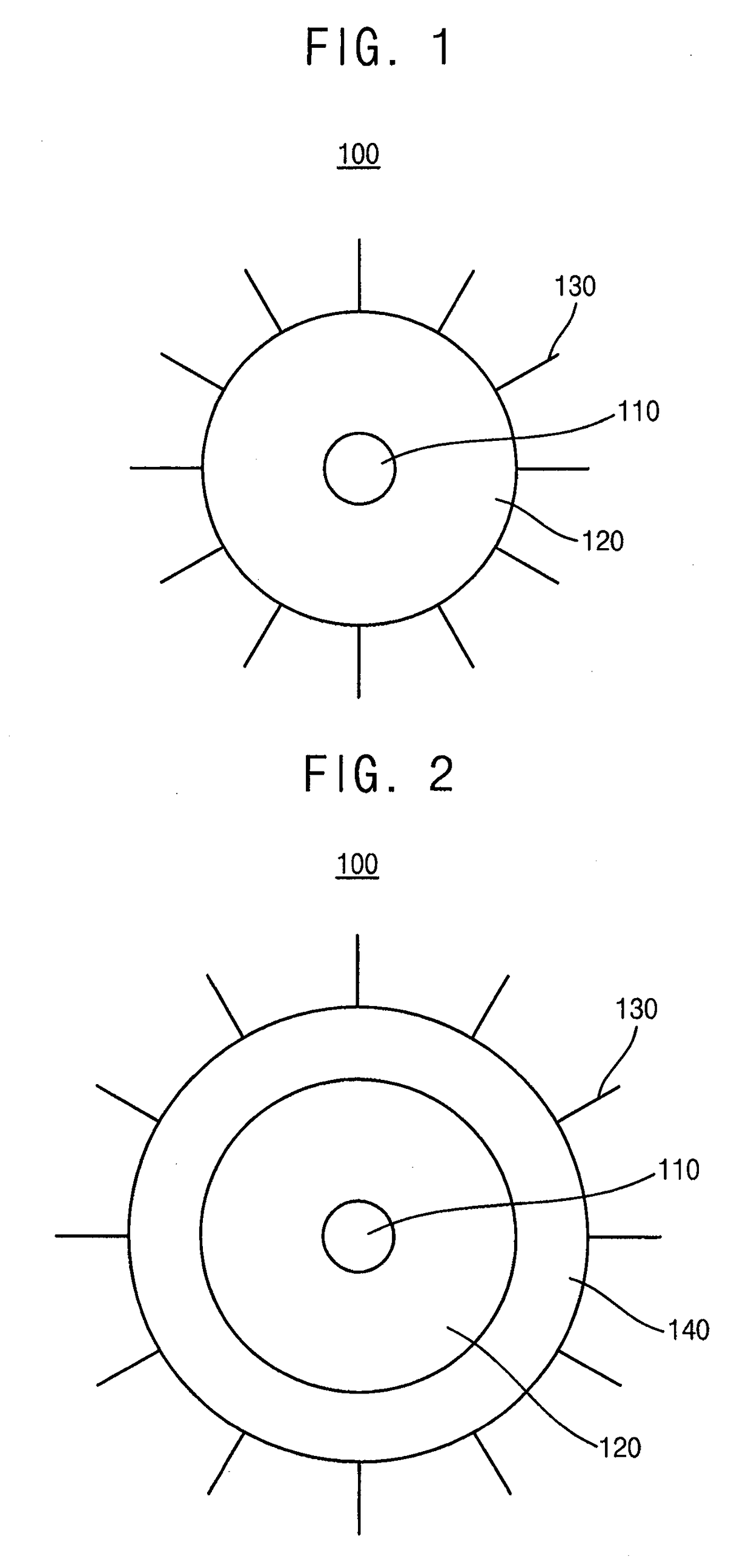
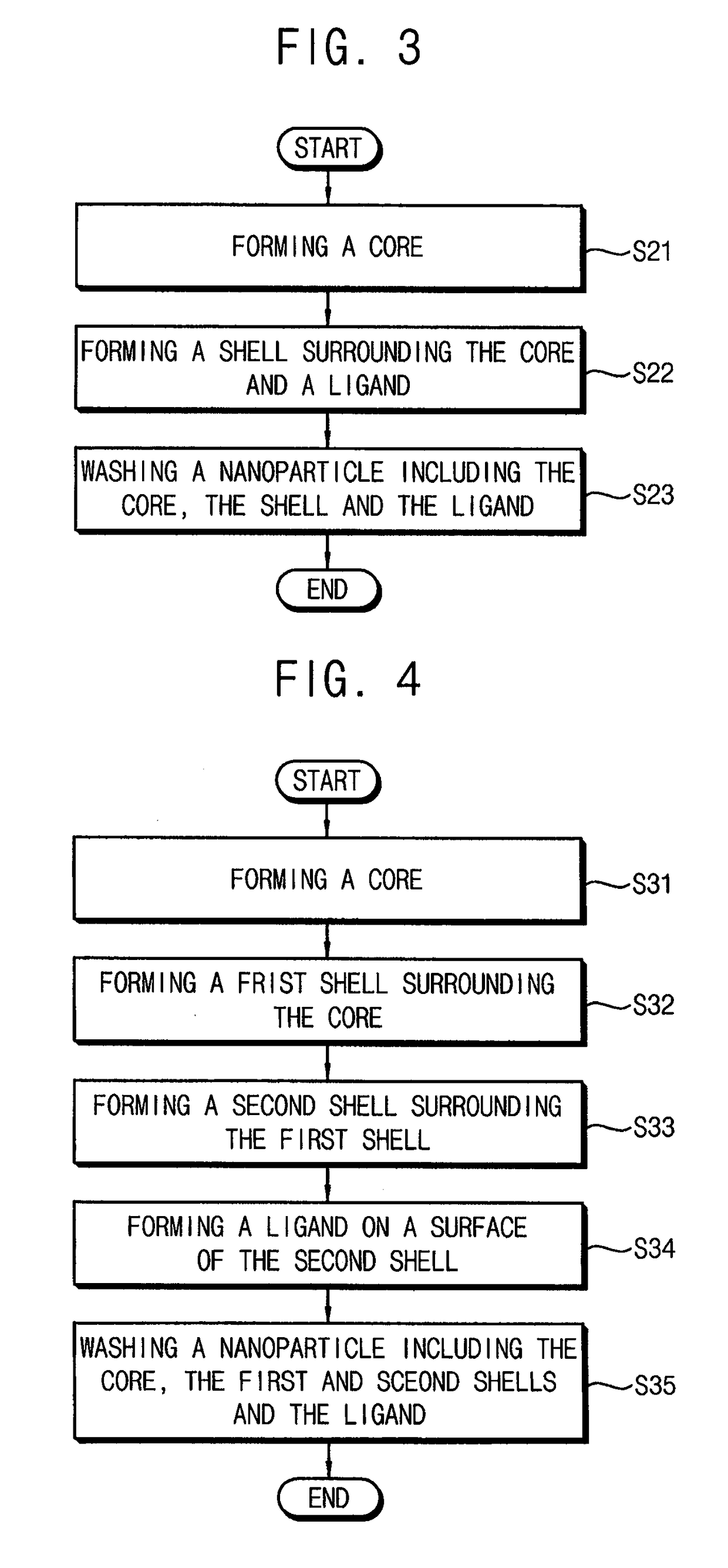
[0096]1 mmol of cadmium oxide and 10 mmol of zinc acetate were added into a three neck flask, and 15 ml of 1-ODE and 7 ml of oleic acid were also added therein to form a first mixture. The first mixture was heated to a temperature of about 150° C. under a vacuum condition, and then heated again to a temperature of about 310° C. under an argon (Ar) atmosphere. 1.6 mmol of sulfur powder was added to 2.4 ml of 1-ODE to form a second mixture, and then the second mixture was added to the heated first mixture to cause a reaction therebetween for about 12 min. Thus, a ZnCdS core was formed. After 4 mmol of sulfur powder was added to 5 ml of oleic acid to form a third mixture, the third mixture was added dropwise onto a surface of the core to cause a react therebetween. The reaction was maintained for about one hour. Hence, a nanoparticle including a ZnS shell or a ZnCdS shell and an oleate ligand was formed. The nanoparticle was precipitated in acetone, and a centrifugal process was perfor...

example 2

[0097]Except that a reaction between a third mixture and a core was maintained for about 2 hours, processes substantially the same as or similar to those of Example 1 were performed to thereby obtain a quantum dot.

example 3

[0098]Except that a reaction between a third mixture and a core was maintained for about 4 hours, processes substantially the same as or similar to those of Example 1 were performed to thereby obtain a quantum dot.


PUM

PropertyMeasurementUnit
sizeaaaaaaaaaa
temperatureaaaaaaaaaa

Abstract

In a method of manufacturing a quantum dot, a core may be formed using (utilizing) at least one cation precursor and at least one anion precursor. The core may be reacted with a shell forming precursor and a ligand forming precursor for more than one hour to form a shell enclosing the core and a ligand. A nanoparticle including the core, the shell and the ligand may be washed.

Description

CROSS-REFERENCE TO RELATED APPLICATIONS[0001]This application is a divisional of U.S. patent application Ser. No. 14 / 244,874, filed Apr. 3, 2014, which claims priority to and the benefit of Korean Patent Application No. 10-2013-0037292, filed on Apr. 5, 2013, in the Korean Intellectual Property Office (KIPO); and Korean Patent Application No. 10-2014-0036760, filed on Mar. 28, 2014, in the Korean Intellectual Property Office, the entire content of each of the patent applications is incorporated herein by reference.BACKGROUND[0002]1. Field[0003]Example embodiments of the invention relate to quantum dots, methods of manufacturing quantum dots and methods of manufacturing organic light emitting display devices using the same.[0004]2. Description of the Related Art[0005]A quantum dot may include a core, a shell surrounding the core, and a ligand chemically bonded to a surface of the shell. The quantum dot may be generally obtained by repeatedly washing a nanoparticle including the core,...

Claims


Application Information

Patent Timeline
Patent Type & Authority Applications(United States)
IPC IPC(8): H01L51/50C09K11/88C09K11/56
CPCH01L51/502C09K11/883C09K11/565H01L51/5072C09K11/025H10K50/115H10K50/16
Inventor KO, HEE-JOOYANG, HEE-SUNLEE, KI-HEONLEE, JEONG-HOONLEE, CHANG-HO
Owner SAMSUNG DISPLAY CO LTD
Why Eureka
Try Eureka