Process for making a CMOS image sensor

a cmos image sensor and processing technology, applied in the field of image sensors, can solve the problems of reducing the quantum efficiency of the image sensor, the possibility of a low success rate, and the optical sensitivity of the image sensor dropping, so as to reduce the increase the quantum efficiency, and reduce the effect of absorption or reflective loss

Inactive Publication Date: 2006-08-10
LAVINE JAMES P
View PDF14 Cites 0 Cited by
  • Summary
  • Abstract
  • Description
  • Claims
  • Application Information

AI Technical Summary

Benefits of technology

[0008] The present invention has the following advantages. Sufficient semi-conducting volume is retained for the image sensor built in SOI to have a quantum efficiency comparable to that of image sensors built in standard semi-conductor wafers. The semi-conducting layer over the photosensitive region may be replaced by a dielectric layer or dielectric layers that permit increased quantum efficiency by the reduction of absorptive or reflective losses in the layers over the photosensitive region.

Problems solved by technology

When CMOS technology is used to fabricate an image sensor, then a tradeoff conflict arises as a shrinking active device volume means the quantum efficiency is severely reduced, i.e., the optical sensitivity of an image sensor drops.
However, thinning is a difficult operation that has the possibility of a low success rate.
Amorphous silicon is a challenging material from which to extract photo-generated carriers, since amorphous silicon generally has a high density of trapping sites for the carriers.
However, the fabrication requires many instances of non-standard process steps.

Method used


Image

  • Process for making a CMOS image sensor
  • Process for making a CMOS image sensor
  • Process for making a CMOS image sensor

Examples


Embodiment Construction

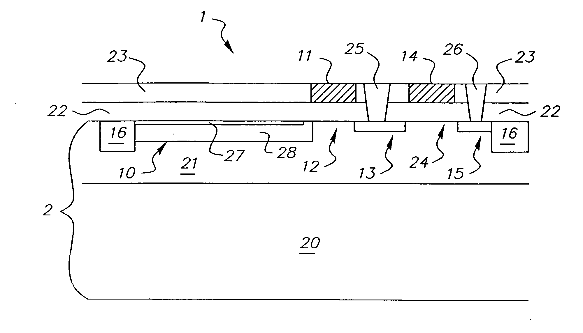
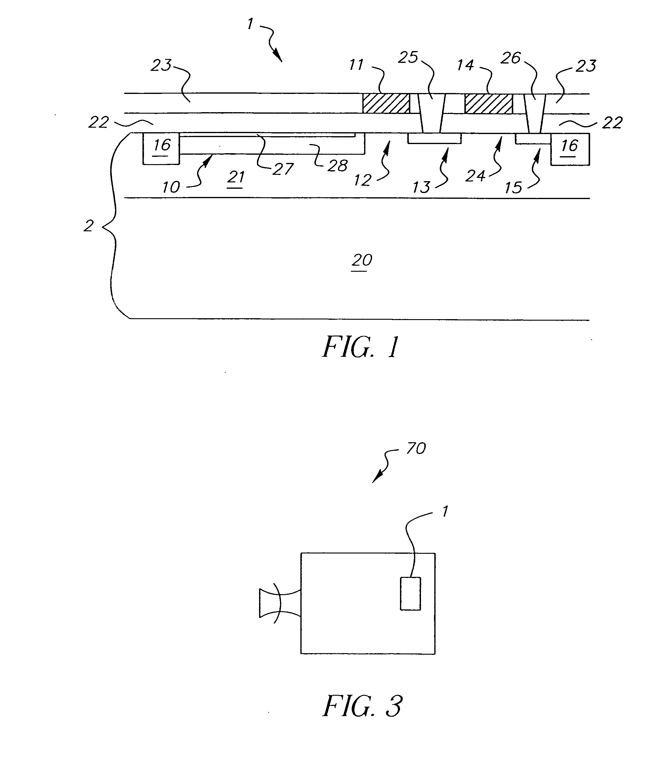
[0012] Referring to FIGS. 1 and 2, there is shown a CMOS image sensor 1 of the present invention. Although a CMOS image sensor is shown as a preferred embodiment, the present invention applies to any suitable image sensor such as a charge coupled device (CCD). The present invention is also preferably implemented on a silicon on insulator wafer which consists of a layer of silicon overlayer 23 on a layer of silicon dioxide 22 which rests on a thick silicon substrate 2. The thick silicon substrate 2 includes two doping regions comprising a first 20 and second layer 21. The second layer region 21 is preferable an epitaxial region. A dielectric layer 22 spans and covers the epitaxial region 21. The silicon overlayer 23 covers and spans the dielectric layer 22. The silicon overlayer 23 is preferably made of a single crystal and is preferably less than 1 micrometer in thickness.

[0013] A pinned photodiode 10 having a p+ layer 27 and an n layer 28 is disposed in the epitaxial layer 21. The...


PUM


Abstract

An image sensor includes a semi-conducting substrate having a photo-sensitive region and doping for forming a path to a charge-to-voltage mechanism; a dielectric spanning the substrate; and a semi-conducting layer, which is less than approximately 1 micrometer, spanning the dielectric which contains electrodes and circuit elements that control flow of charge.

Description

CROSS-REFERENCE TO RELATED APPLICATIONS [0001] This is a divisional of application Ser. No. 10 / 753,246, filed Jan. 8, 2004.FIELD OF THE INVENTION [0002] The invention relates to the field of image sensors and, more particularly, to making an image sensor in a wafer that has the structure of a semi-conductor layer over a dielectric layer that is over a semi-conducting substrate. More specifically, the invention relates to making an image sensor with the photosensitive region in the semi-conducting substrate and most of the signal transport and processing circuits in the semi-conducting layer. BACKGROUND OF THE INVENTION [0003] CMOS technology continues to have a trend of finer dimensions with shallower active device volumes. When CMOS technology is used to fabricate an image sensor, then a tradeoff conflict arises as a shrinking active device volume means the quantum efficiency is severely reduced, i.e., the optical sensitivity of an image sensor drops. This trend is most clearly see...

Claims


Application Information

Patent Timeline
Patent Type & Authority Applications(United States)
IPC IPC(8): H01L21/00H01L27/00
CPCH01L27/14632H01L27/14687
Inventor LAVINE, JAMES P.
Owner LAVINE JAMES P
Why Eureka
Try Eureka