LCD device with improved optical performance

a liquid crystal display and optical performance technology, applied in static indicating devices, non-linear optics, instruments, etc., can solve problems such as inability to use, and achieve the effect of reducing voltage potential

Active Publication Date: 2006-12-21
AU OPTRONICS CORP
View PDF13 Cites 85 Cited by
  • Summary
  • Abstract
  • Description
  • Claims
  • Application Information

AI Technical Summary

Benefits of technology

[0006] In a liquid crystal display (LCD) panel having a plurality of pixels, each having a first electrode connected to a common line, a second electrode connected to a data line through an TFT and a charge storage capacitor connected to the second electrode at the first capacitor end, the voltage applied to the second capacitor end is equal the voltage at the common line, or Vcom. After the gate line signal has passed, a reduction in the voltage potential between the first and second electrodes occurs. This voltage reduction is known as the feed-through potential drop. In order to compensate for this voltage potential reduction, the voltage applied to the second end of the charge storage capacitor is increased from Vcom to Vcom1 after the gate line signal has passed. This applied voltage adjustment can be achieved by using two switching elements connected to the second end of the charge storage capacitor. One switching element is activated by the gate line signal so that the applied voltage is equal to Vcom. The other switching element is activated by the next gate line signal so that the applied is increased to Vcom1.

Problems solved by technology

This three-step gate-line signal is useful only when the storage capacitors Cst are tied to the gate lines, but it cannot be used when the storage capacitors Cst are tied to the common lines.

Method used


Image

  • LCD device with improved optical performance
  • LCD device with improved optical performance
  • LCD device with improved optical performance

Examples


Embodiment Construction

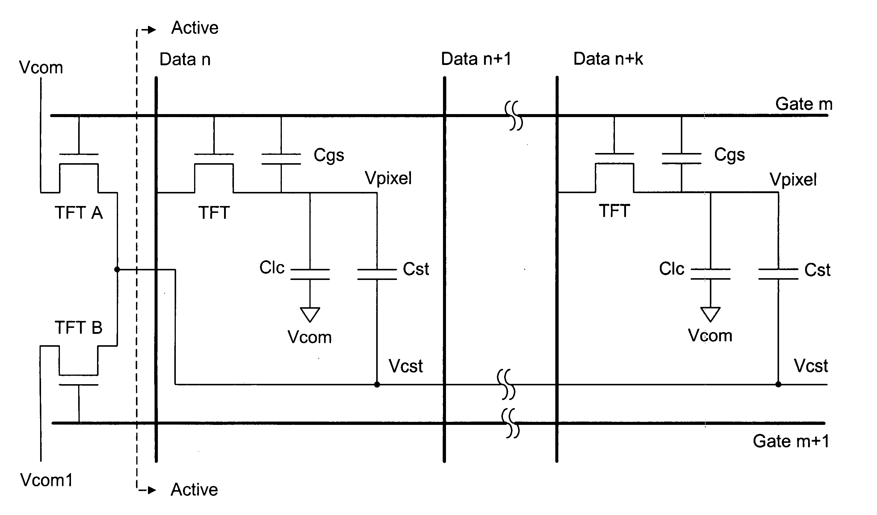
[0037] The present invention makes use of different signal levels in the common line voltages to compensate for the feed-through potential drop. As with prior art, the voltage potential associated with the charge capacity Clc is determined by the pixel voltage Vpixel and the signal level Vcom at a common line. In contrast to prior art, the voltage on one end of the additional charge storage capacitor Cst is switched between Vcom and Vcom1 as shown in FIG. 5. In one embodiment of the present invention, these voltage levels are controlled by TFT A and TFT B before the signal line VCst enters the active area of the LCD device. As shown in FIG. 6, when the signal level at gate line m is high (gate line m+1 being at Vgl), the switching TFT A and TFT are in the “ON” state but TFT B is “OFF”. The voltage potential across Clc is (Vdata−Vcom) and the voltage across Cst is also (Vdata−Vcom). The voltage potential across Cgs is (Vdata−Vgh). The total charge on these capacitors is

Qpixel=(Clc+C...


PUM


Abstract

In an LCD pixel, the pixel voltage is usually reduced after a gate line signal has passed. To compensate for this voltage reduction, the voltage applied to the charge storage capacitor in the pixel is increased from Vcom to Vcom1 after the gate line signal has passed. Voltage adjustment can be achieved by using two switching elements connected to the second end of the charge storage capacitor. One is activated by the gate line signal so that the applied voltage is equal to Vcom, and the other is activated by the next gate line signal so that the applied is increased to Vcom1. In a transflective LCD panel or a color LCD panel, each pixel is divided into two or three sub-pixels, each sub-pixel having a separate charge storage capacitor, a similar Vcom change is applied to each of the charge storage capacitors in the pixel.

Description

FIELD OF THE INVENTION [0001] The present invention relates to a liquid crystal display and, in particular, to a liquid crystal display with reduced feed-through potential drop. BACKGROUND OF THE INVENTION [0002] In a liquid crystal display comprising a plurality of gate lines and data lines, and an array of pixels arranged between adjacent gates lines and data lines, it is desirable to maintain the voltage potential on a pixel (m, n) over a reasonable period of time after the signal at the gate-line has changed from an H-state (Vgh) to an L-state (Vgl). The voltage potential is maintained by the charge capacity of each pixel. The charge is partially stored in the liquid crystal layer between the pixel electrodes, one of which is connected to a common electrode and the other is connected to the data line n through a switching element. As shown in FIG. 1, the charge capacity associated with the liquid crystal layer is represented by Clc, and the switching element is a TFT. In order t...

Claims


Application Information

Patent Timeline
Patent Type & Authority Applications(United States)
IPC IPC(8): G09G3/36
CPCG02F1/136213G02F2203/09G02F2203/21G09G3/2011G09G2320/0204G09G3/3655G09G2300/0443G09G2300/0456G09G2300/0876G09G3/3648
Inventor HUANG, HSUEH-YING
Owner AU OPTRONICS CORP
Why Eureka
Try Eureka