Method for adhesion and deposition of metal films which provide a barrier and permit direct plating

a metal film and barrier technology, applied in the direction of basic electric elements, semiconductor/solid-state device manufacturing, electric devices, etc., can solve the problems of resist poisoning problems, metals do not adhere well,

Inactive Publication Date: 2006-12-21
INTEL CORP
View PDF5 Cites 13 Cited by
  • Summary
  • Abstract
  • Description
  • Claims
  • Application Information

AI Technical Summary

Problems solved by technology

Unfortunately, in many cases these metals do not adhere well to, for instance, an underlying dielectric layer.
Moreover, TaN depositions have inherent resist poisoning problems.

Method used


Image

  • Method for adhesion and deposition of metal films which provide a barrier and permit direct plating
  • Method for adhesion and deposition of metal films which provide a barrier and permit direct plating
  • Method for adhesion and deposition of metal films which provide a barrier and permit direct plating

Examples


Embodiment Construction

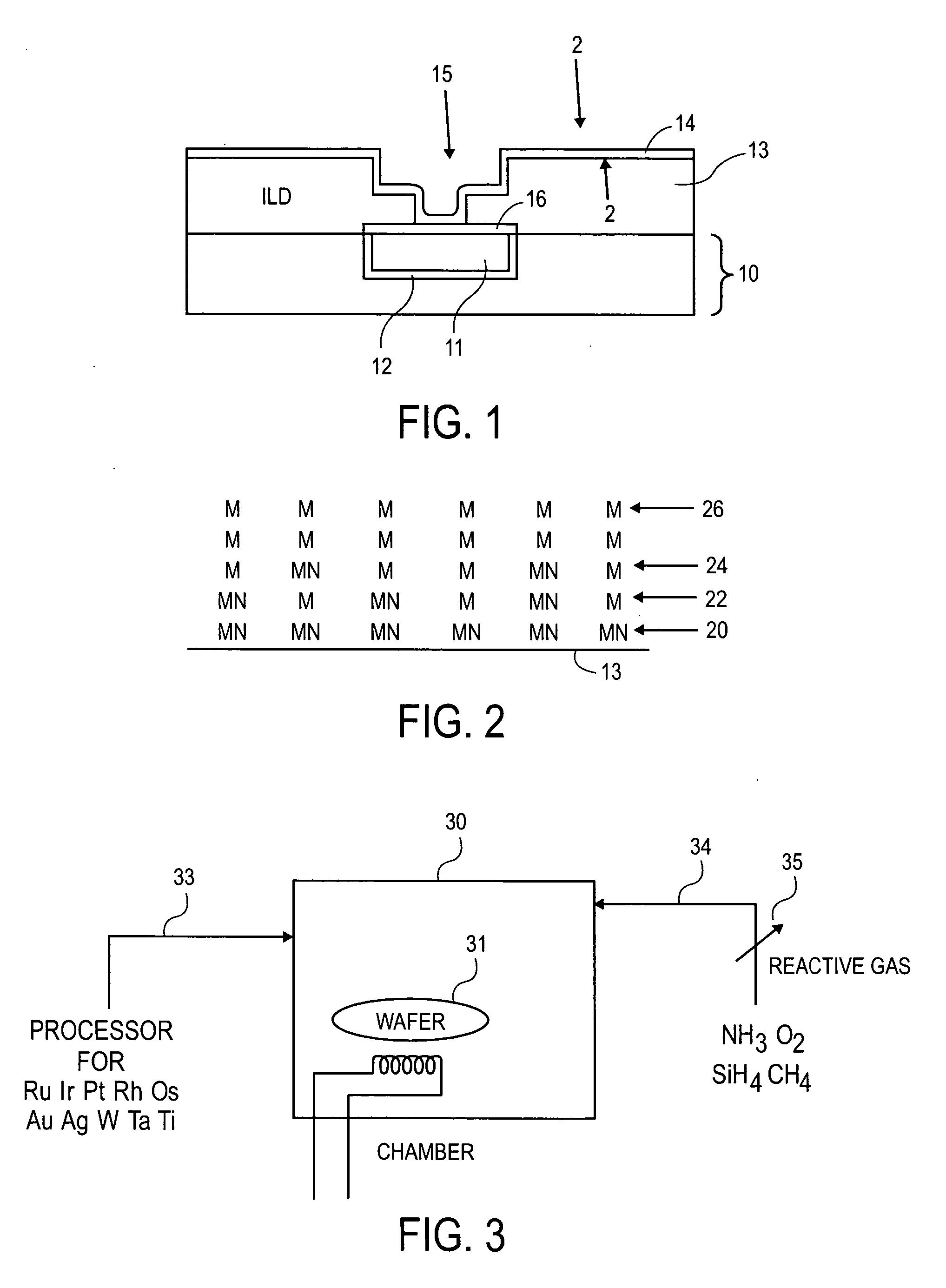
[0008] A method and layer are described for providing a barrier layer which enables direct plating without a separate seed layer. In the following description, numerous specific details are set forth such as specific precursors, in order to provide a thorough understanding of the present invention. It will be apparent to one skilled in the art, that the process described may be practiced without these specific details. In other instances, well-known processing steps, such as etching and cleaning steps, are not described in detail in order to not unnecessarily obscure the description which follows.

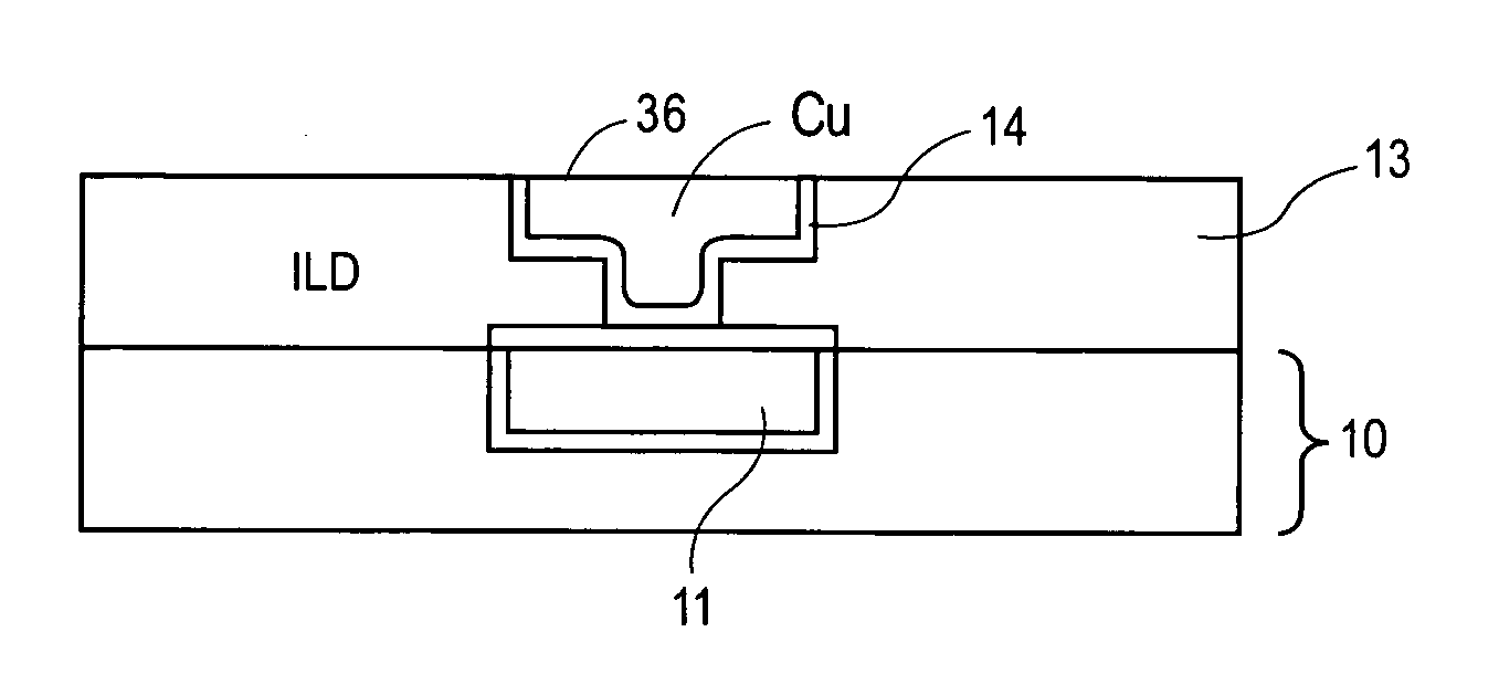
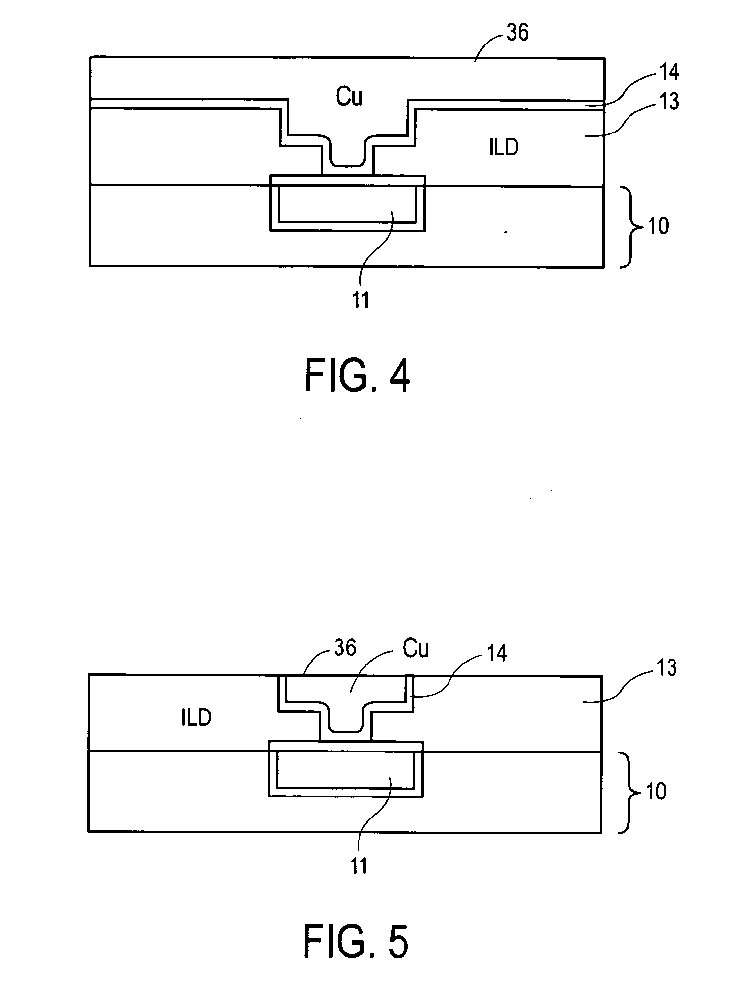
[0009] In FIG. 1, a first interconnect level 10 is shown having a conductor 11 lined with a barrier layer 12 and capped with a capping layer 16. By way of example, the conductor 11 may be a copper or copper alloy conductor lined with a typical barrier metal such as a TaN, and capped with a selectively deposited cobalt layer 16. The barrier layer 12 may instead be a barrier layer such as de...


PUM

PropertyMeasurementUnit
structureaaaaaaaaaa
dielectricaaaaaaaaaa
adhesionaaaaaaaaaa

Abstract

A method for fabricating a barrier layer and a barrier layer is described which employs a metal selected from the group of Ru, Ir, Pd, Pt, Rh, Os, Au, Ag, W, Ta and Ti. A graded region is formed to cause the metal to adhere to an underlying substrate. Direct plating is enabled without a seed layer.

Description

FIELD OF THE INVENTION [0001] The invention related to forming of barrier layers and seed layers in semiconductor processing such as are used in a damascene process. PRIOR ART AND RELATED ART [0002] Some thin metal films, including certain noble metals, have been identified as key enablers for permitting direct plating onto a barrier layer, thereby eliminating a separate seed layer. This is discussed in “Forming a Copper Diffusion Barrier,” Pub. No. US2004 / 0084773. Unfortunately, in many cases these metals do not adhere well to, for instance, an underlying dielectric layer. The use of a more standard barrier, such as TaN, underlying the noble metal layer provides adhesion but at the cost of the complexities associated with forming the TaN layer. Moreover, TaN depositions have inherent resist poisoning problems. BRIEF DESCRIPTION OF THE DRAWINGS [0003]FIG. 1 is a cross-section, elevation view of a semiconductor substrate showing an underlying conductor and an opening in an interlayer...

Claims


Application Information

Patent Timeline
Patent Type & Authority Applications(United States)
IPC IPC(8): H01L21/44
CPCH01L21/76826H01L21/76846H01L21/76831
Inventor DOMINGUEZ, JUAN E.MCSWINEY, MICHAEL L.JOHNSTON, STEVEN W.
Owner INTEL CORP
Why Eureka
Try Eureka