CMOS image sensor and manufacturing method thereof

a metal oxide semiconductor and image sensor technology, applied in the direction of diodes, semiconductor devices, radiation control devices, etc., can solve the problems of reducing the yield affecting the uniformity of the microlenses on the entire wafer, and complicated manufacturing process of the ccd, so as to improve the yield and reliability of the image sensor, improve the uniformity of the surface tension, and improve the evenness of the microlenses

Inactive Publication Date: 2006-12-28
DONGBU ELECTRONICS CO LTD
View PDF8 Cites 3 Cited by
  • Summary
  • Abstract
  • Description
  • Claims
  • Application Information

AI Technical Summary

Benefits of technology

[0018] An object of the present invention is to provide a CMOS image sensor and a manufacturing method thereof for increasing the evenness of a microlens by correcting the uniformities of surface tensions of a planarizing layer during its hardening process, and increasing yield and reliability of the image sensor by preventing defects of the microlens.

Problems solved by technology

Since the CCD has a complicated driving method, consumes much power, and requires a multi-step photolithography process, the manufacturing process of the CCD is complicated.
Consequently, the reflow ability of the microlens pattern formed on the planarizing layer becomes uneven, and the formation of the microlenses in a uniform state on the entire wafer becomes difficult.
When the unevenness (of regions A and B) is severe, a defective microlens is formed, decreasing yield of the image sensor.

Method used


Image

  • CMOS image sensor and manufacturing method thereof
  • CMOS image sensor and manufacturing method thereof
  • CMOS image sensor and manufacturing method thereof

Examples


Embodiment Construction

[0025] Reference will now be made in detail to the preferred embodiments of the present invention, examples of which are illustrated in the accompanying drawings.

[0026]FIGS. 2A through 2D are sectional views showing a manufacturing process of a CMOS image sensor according to an embodiment of the present invention.

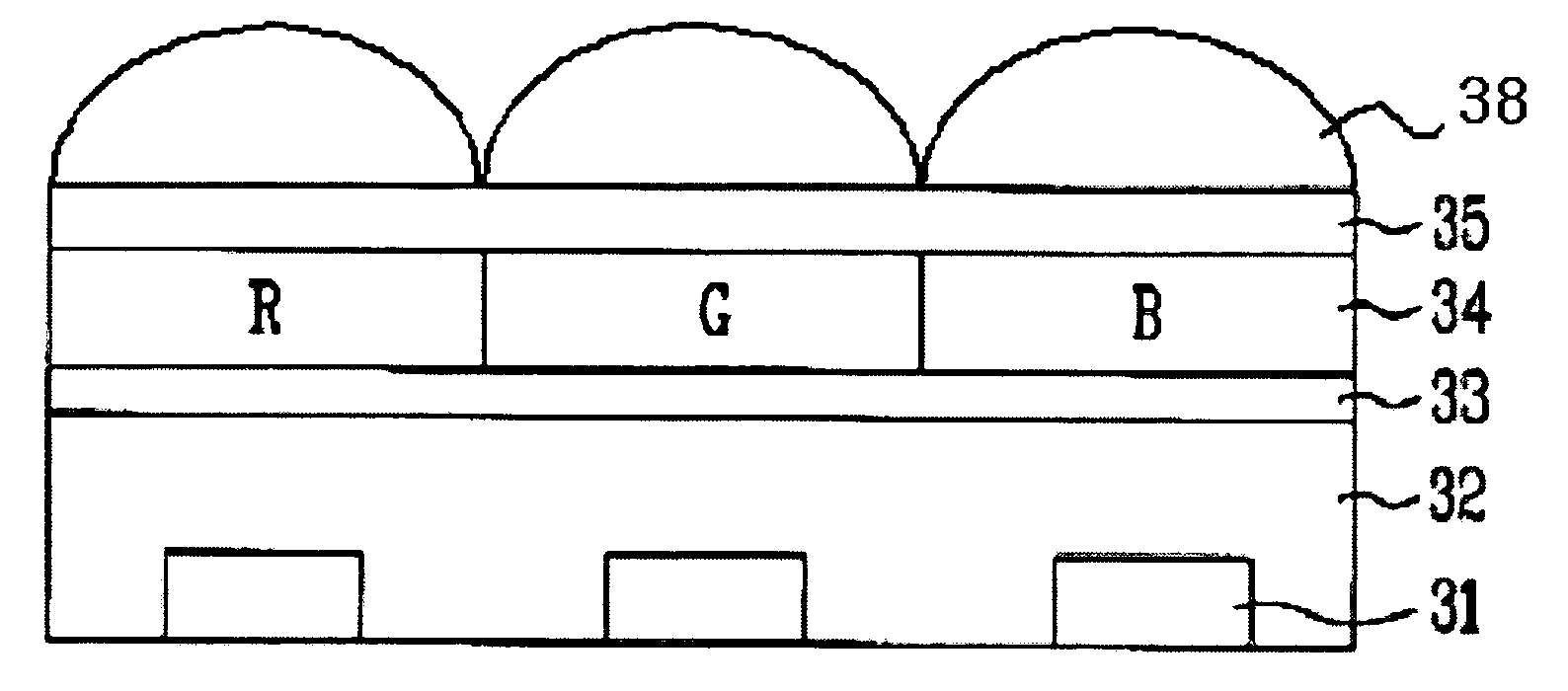
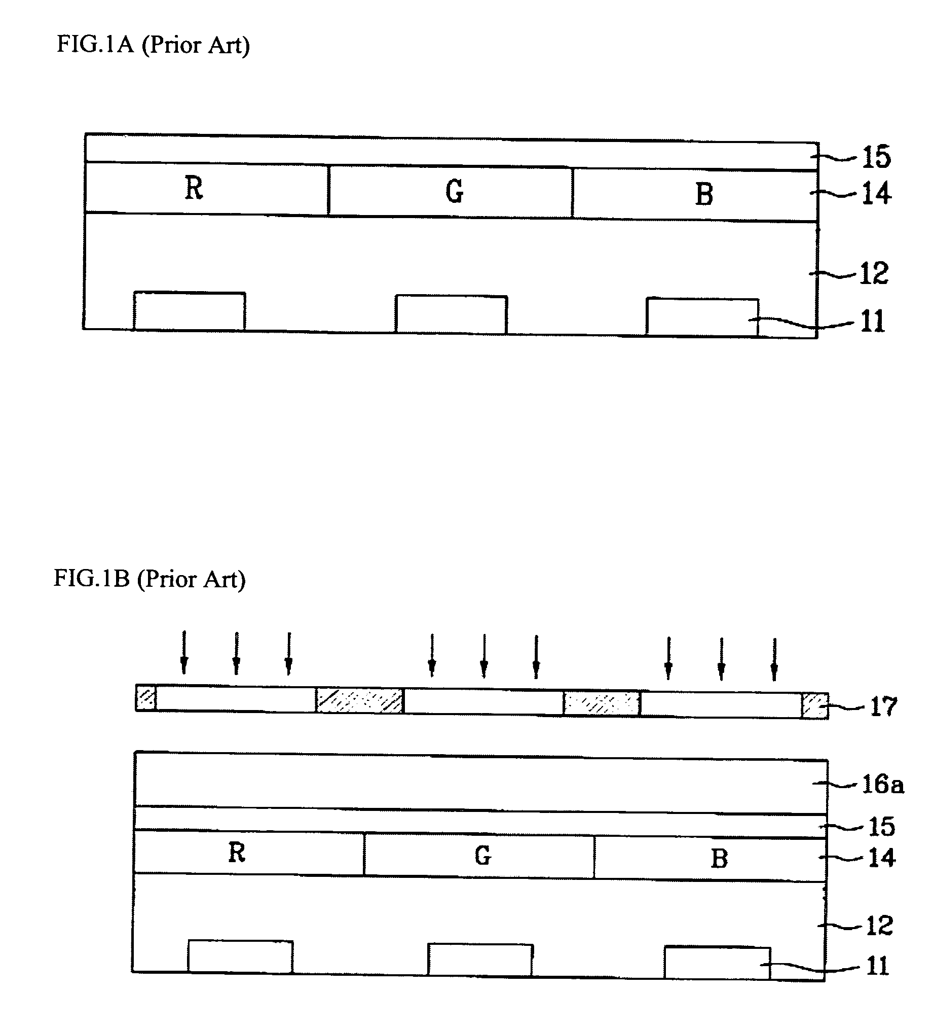
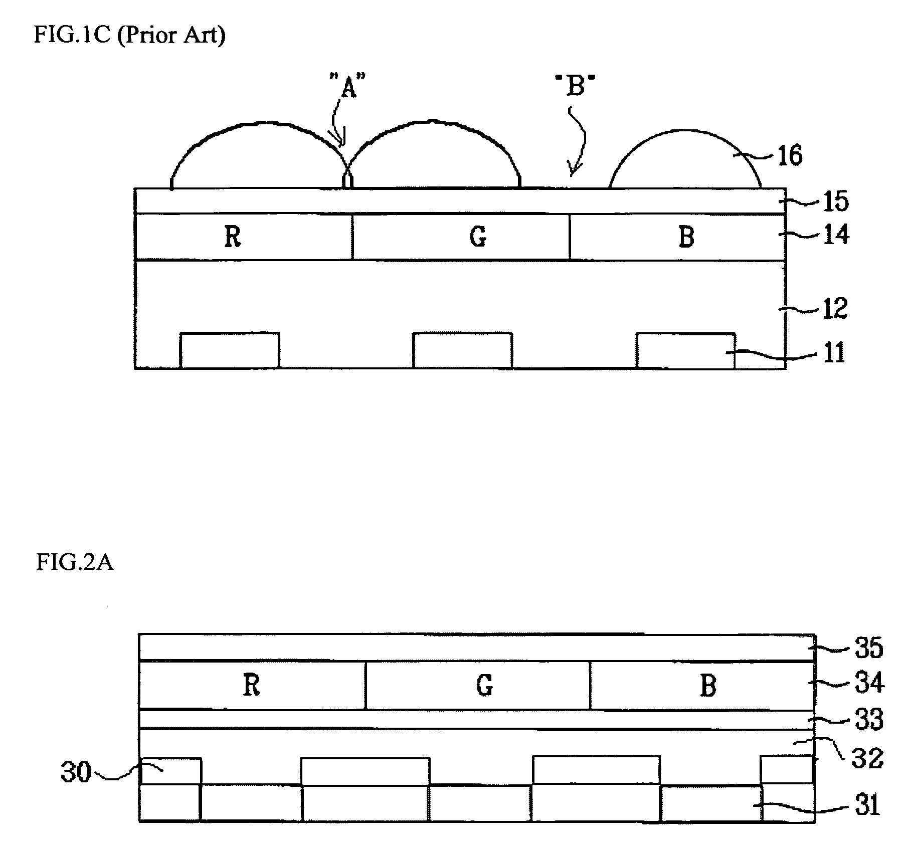
[0027] Referring to FIG. 2A, an interlayer insulating layer 32 is formed over the entire surface of a semiconductor substrate with one or more photodiodes 31 formed thereon. The photodiodes 31 generate a charge according to the amount of incident light and can be formed by any known methods.

[0028] In one embodiment, the interlayer insulating layer 32 can be formed as a multi layer. In another embodiment, the interlayer insulating layer 32 can incorporate a light blocking layer 30 for blocking incident light between photodiode regions. In such an embodiment, a first interlayer insulating layer can be formed on the substrate and photodiodes 31, upon which the light blockin...


PUM


Abstract

Provided are a CMOS image sensor and a manufacturing method thereof. The CMOS image sensor incorporates an interlayer insulating layer, a color filter layer, a first planarizing layer, and at least one microlens. The interlayer insulating layer is formed on a semiconductor substrate having at least one photodiode. The color filter layer is formed above the interlayer insulating layer and incorporates at least one color filter. The first planarizing layer is formed on the color filter layer, and has a uniform surface tension from being UV radiated after a hardening process. The at least one microlens is formed on the first planarizing layer to correspond to the at least one photodiode.

Description

RELATED APPLICATION [0001] This application claims the benefit under 35 U.S.C. §119(e) of Korean Patent Application Number 10-2005-0055590, filed Jun. 27, 2005, which is incorporated herein by reference in its entirety. FIELD OF THE INVENTION [0002] The present invention relates to a complementary metal oxide semiconductor (CMOS) image sensor and a manufacturing method thereof. BACKGROUND OF THE INVENTION [0003] In general, an optical image sensor is a semiconductor device that converts an optical image into an electrical signal. Optical image sensors are roughly classified into charge coupled devices (CCDs) and complementary metal oxide semiconductors (CMOSs). [0004] Since the CCD has a complicated driving method, consumes much power, and requires a multi-step photolithography process, the manufacturing process of the CCD is complicated. In order to overcome the drawbacks of the CCD, the CMOS image sensor is favored as a next generation image sensor in the industry. [0005] A CMOS i...

Claims


Application Information

Patent Timeline
Patent Type & Authority Applications(United States)
IPC IPC(8): H01L31/113
CPCH01L27/14627H01L27/14685H01L27/14643H01L27/14632H01L27/146
Inventor SIK, KIM SANG
Owner DONGBU ELECTRONICS CO LTD
Why Eureka
Try Eureka