Method to control flatband/threshold voltage in high-k metal gated stacks and structures thereof

a technology of metal gate stacks and flatband/threshold voltage, which is applied in the field of semiconductor structures, can solve the problems of non-ideal threshold voltage of mosfets fabricated with hafnium oxide as the gate dielectric, and achieve the effect of promoting the necessary flatband voltage shift and altering the effective alignment of the workfunctions of the material stack

Inactive Publication Date: 2006-12-28
GLOBALFOUNDRIES INC
View PDF46 Cites 62 Cited by
  • Summary
  • Abstract
  • Description
  • Claims
  • Application Information

AI Technical Summary

Benefits of technology

[0022] If a small quantity of alkaline earth metal is present, the alkaline earth metal ion substituting for the metal ion of the high k dielectric, e.g., Hf, acts as a negatively charged defect (REmetal-). Due to needs for charge neutrality, the presence of the alkaline earth metal substitutional defect can raise the concentration of the charged oxygen vacancies, thereby promoting the necessary flatband voltage shift. Thirdly, via its strong electropositive nature, the alkaline earth metal atom will modify the interface chemistry at the semiconductor / chemox / high k dielectric interfacial region and the top high k dielectric / alkaline earth metal-containing / electrically conductive capping layer region altering the effective alignment of the workfunctions of the material stack. In essence, all three of the aforementioned phenomena are the consequence of insertion of a highly electropositive element as a distinct layer in the stack sequence. This distinct layer then can interdiffuse, but the presence of a composition profile for this electropositive element ensures the flatband / threshold voltage.

Problems solved by technology

It is emphasized that prior art Si MOSFETs fabricated with hafnium oxide as the gate dielectric suffer from a non-ideal threshold voltage when n-MOSFETs are fabricated.

Method used


Image

  • Method to control flatband/threshold voltage in high-k metal gated stacks and structures thereof
  • Method to control flatband/threshold voltage in high-k metal gated stacks and structures thereof
  • Method to control flatband/threshold voltage in high-k metal gated stacks and structures thereof

Examples


example

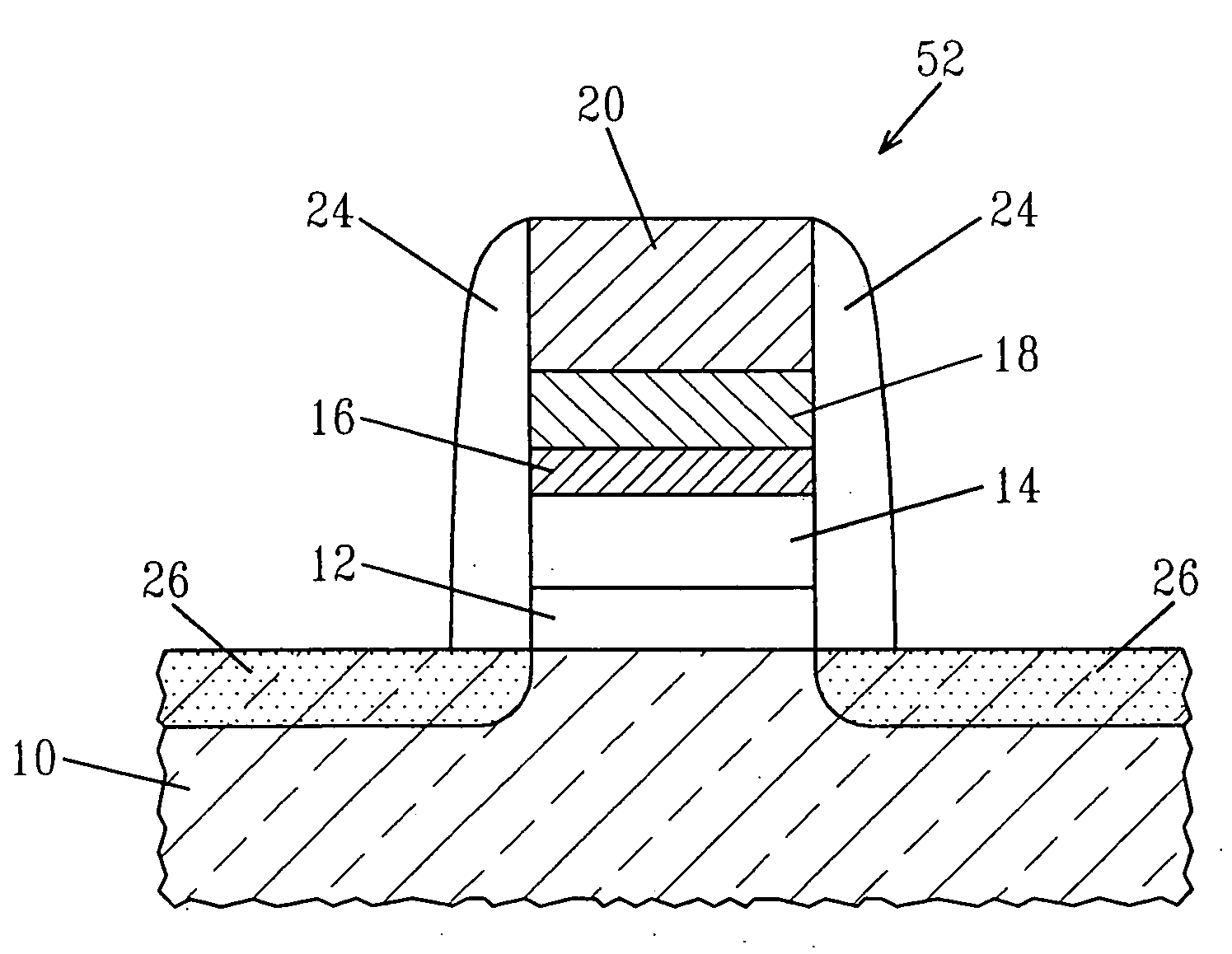
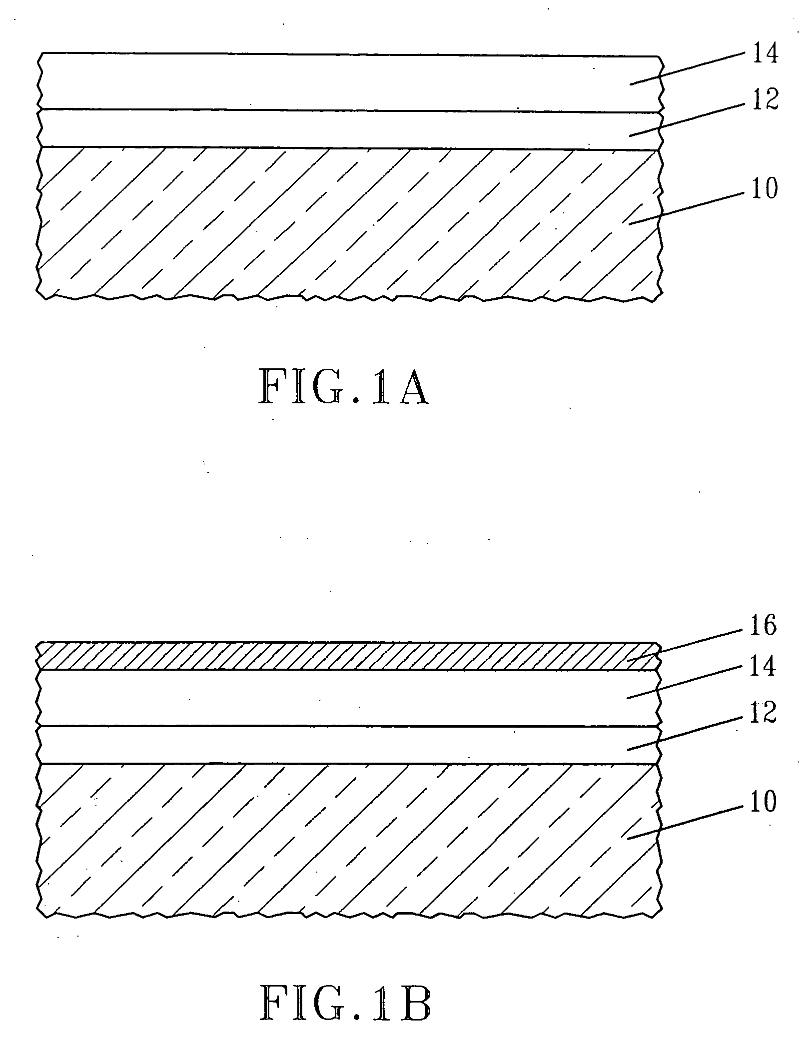
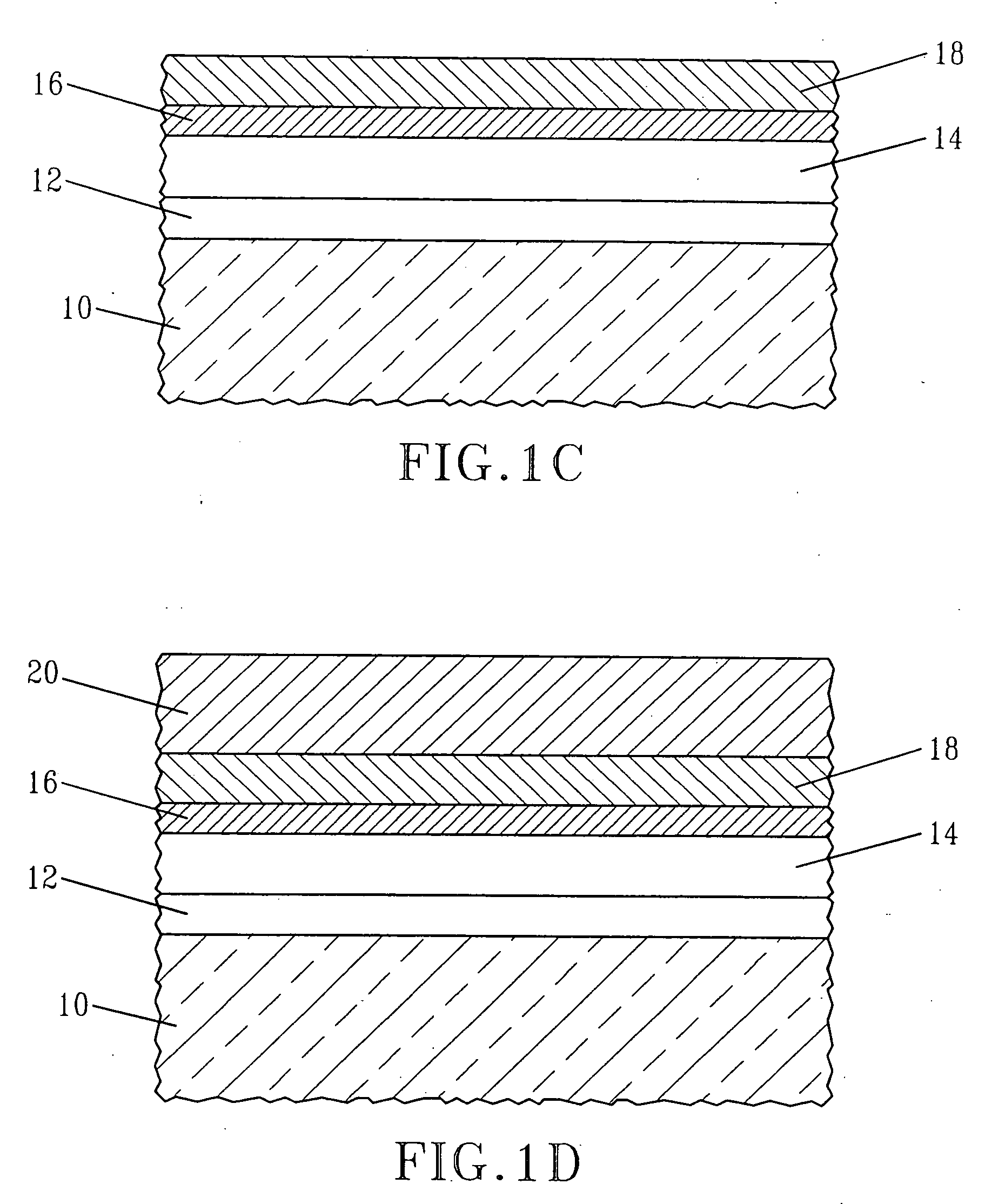
[0057] In this example, MOSCAPs were prepared utilizing material stacks of the present invention and they were compared with a prior art MOSCAP which did not include the inventive material stack. Specifically, material stacks comprising HfO2 / 5 Å MgO / TiN / PolySi stack (Inventive 1) and HfSiO / 5 Å MgO / TiN / PolySi stack (Inventive 2) were prepared utilizing the processing steps mentioned above and those material stack were used as a component of a MOSCAP. A prior art material stack, including HfO2, but not including MgO, was prepared and was used a component for a prior art MOSCAP (Prior Art). Each material stack after processing was subjected to a 1000° C. rapid thermal anneal in nitrogen, followed by a 500° C. forming gas anneal.

[0058]FIG. 3 shows the CV curves of these MOSCAPs. The CET (Capacitance Equivalent Thickness) of the Inventive material stack 1 was 13 Å, while the CET for Inventive material stack 2 was 15 Å. The CET of the Prior Art material stack was 14.5 Å.

[0059] The flatb...


PUM


Abstract

The present invention provides a metal stack (or gate stack) structure that stabilizes the flatband voltage and threshold voltages of material stacks that include a gate conductor and a dielectric material having a dielectric constant of greater than about 4.0, especially a Hf-based dielectric. This present invention stabilizes the flatband voltages and the threshold voltages by introducing an alkaline earth metal-containing layer into the material stack that introduces, via electronegativity differences, a shift in the threshold voltage to the desired voltage. Specifically, the present invention provides a metal stack comprising a high k dielectric, preferably a hafnium-based dielectric; an alkaline earth metal-containing layer located atop of, or within, said high k dielectric; an electrically conductive capping layer located above said high k dielectric; and a gate conductor.

Description

RELATED APPLICATIONS [0001] This application is related to co-pending and co-assigned U.S. application Ser. No. 11 / 118,521, filed Apr. 29, 2005, the entire content of which is incorporated herein by reference.FIELD OF THE INVENTION [0002] The present invention generally relates to a semiconductor structure, and more particularly to a material stack useful in metal oxide semiconductor capacitors (MOSCAPs) and metal oxide semiconductor field effect transistors (MOSFETs) that includes an alkaline earth metal-containing material present on top of, or within, a high k dielectric layer which is capable of stabilizing the threshold voltage and flatband voltage of a gate conductor. Specifically, the presence of the alkaline earth metal-containing material induces a band bending in a semiconductor substrate so as to shift the threshold voltage to more negative values than when such a layer is not used. BACKGROUND OF THE INVENTION [0003] In standard silicon complementary metal oxide semicondu...

Claims


Application Information

Patent Timeline
Patent Type & Authority Applications(United States)
IPC IPC(8): H01L29/94
CPCH01L21/28088H01L21/28167H01L21/28194H01L29/78H01L29/513H01L29/517H01L29/4966
Inventor BROWN, STEPHEN L.CHEN, TZE-CHIANGJAMMY, RAJARAONARAYANAN, VIJAYPARUCHURI, VAMSI K.
Owner GLOBALFOUNDRIES INC
Why Eureka
Try Eureka