High speed output buffer with AC-coupled level shift and DC level detection and correction

Inactive Publication Date: 2007-01-04
NORTH STAR INNOVATIONS
View PDF33 Cites 25 Cited by
  • Summary
  • Abstract
  • Description
  • Claims
  • Application Information

AI Technical Summary

Problems solved by technology

Current Input/Output (I/O) architectures rely on higher voltage, thick gate-oxide devices (e.g., Dual-Gate Oxide (DGO) devices and the like) to implement output drivers for safe operation, yet such drivers suffer from low performance particularly at lower voltage levels of the chip.
The proc

Method used


Image

  • High speed output buffer with AC-coupled level shift and DC level detection and correction
  • High speed output buffer with AC-coupled level shift and DC level detection and correction
  • High speed output buffer with AC-coupled level shift and DC level detection and correction

Examples


Embodiment Construction

[0018] The following description is presented to enable one of ordinary skill in the art to make and use the present invention as provided within the context of a particular application and its requirements. Various modifications to the preferred embodiment will, however, be apparent to one skilled in the art, and the general principles defined herein may be applied to other embodiments. Therefore, the present invention is not intended to be limited to the particular embodiments shown and described herein, but is to be accorded the widest scope consistent with the principles and novel features herein disclosed.

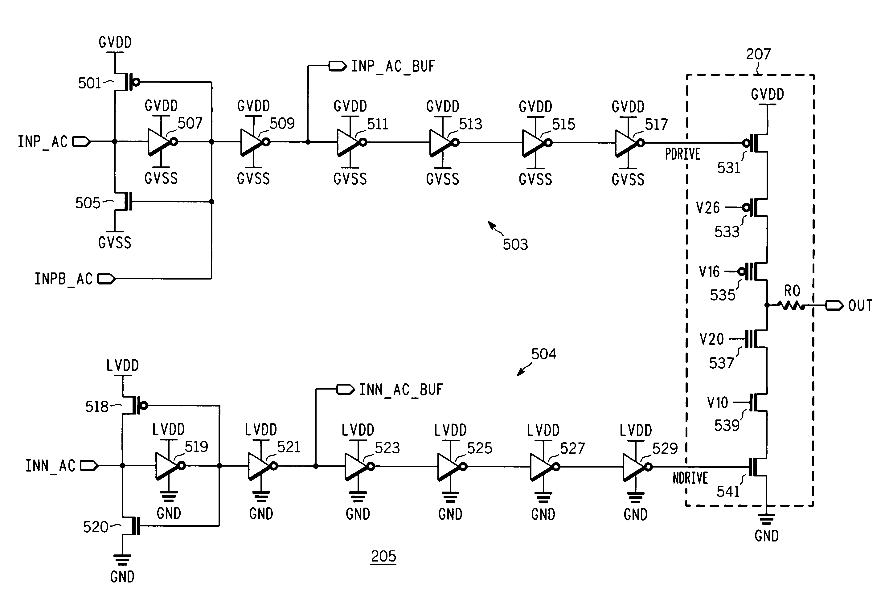
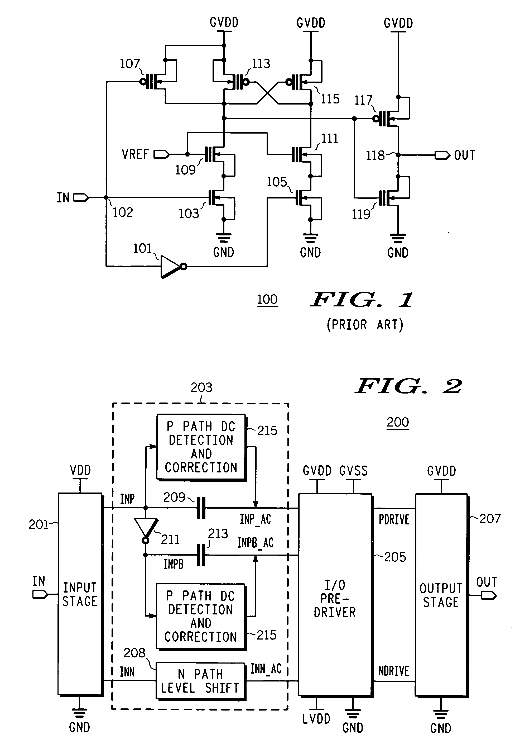
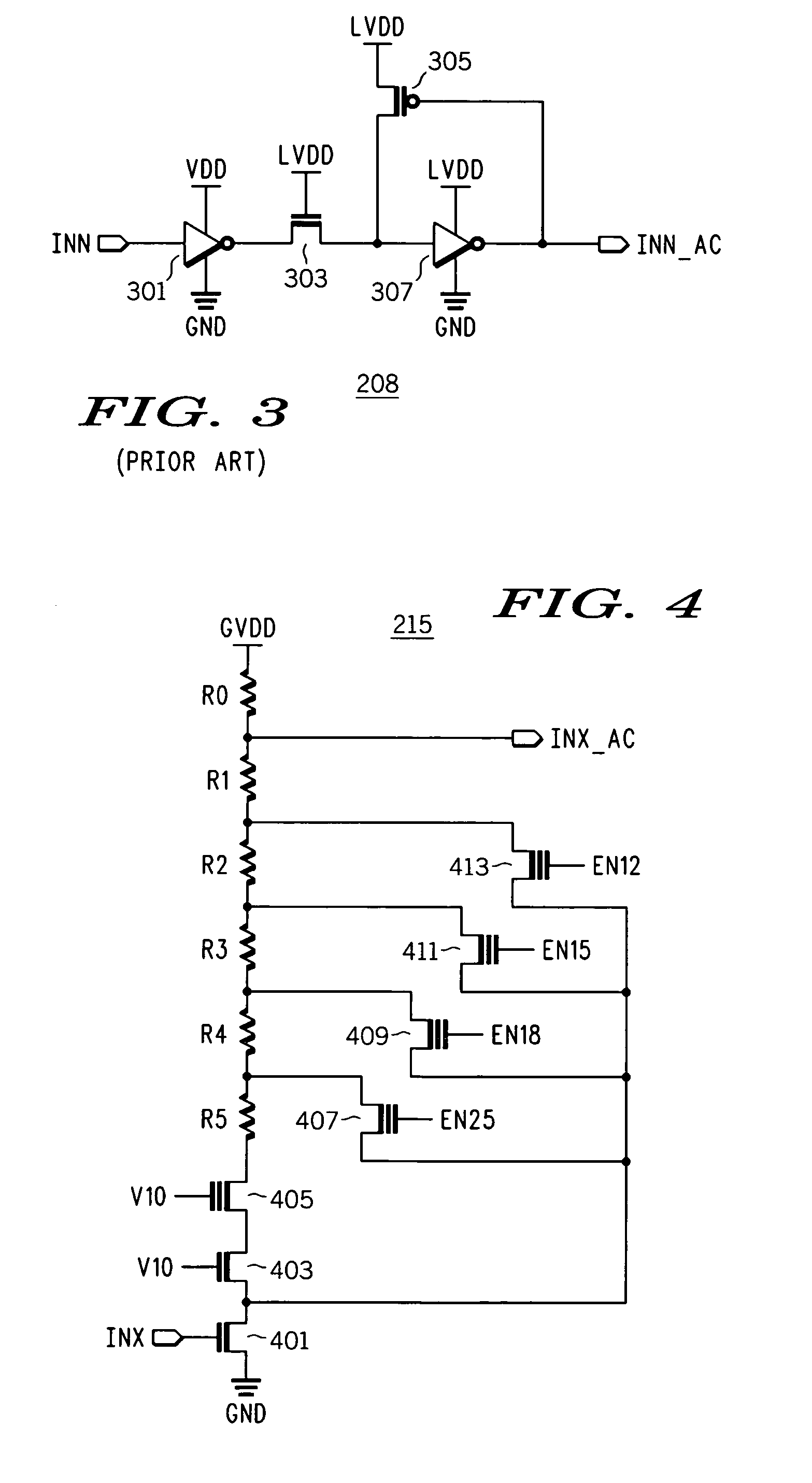
[0019]FIG. 1 is a schematic diagram of a level shifter 100 implemented using CMOS technology according to prior art which level shifts a lower input voltage to a higher output voltage suitable for a conventional pre-driver circuit (not shown). An input signal IN is provided to an input node 102, which is coupled to the input of an inverter 101, to the gate of an N-channel tra...


PUM


Abstract

A high speed output buffer including an input circuit providing first and second signals within a first voltage range having a first common mode voltage, an AC interface receiving the first and second signals and providing first and second preliminary drive signals, a detection and correction circuit that corrects a state of the first preliminary drive signal AC coupled to the first signal, first and second drive circuits receiving the preliminary drive signals and providing first and second drive signals, where the first drive circuit operates within a second voltage range having a greater common mode voltage and where the second drive circuit operates within a third voltage range, and an output that switches an output node within a voltage range that is greater than a maximum voltage range. The first, second and third voltage ranges are each within the maximum voltage range suitable for thin-gate devices.

Description

BACKGROUND OF THE INVENTION [0001] 1. Field of the Invention [0002] The present invention relates in general to electronic devices, and more specifically to a high speed output driver with internal AC-coupled level shift and DC level detection and correction. [0003] 2. Description of the Related Art [0004] Process technologies, including CMOS processes, are continually improving resulting in smaller and faster devices, such as, for example, 90-nm (nanometer) CMOS. Yet many systems include circuitry designed with a variety of technologies operating at multiple voltage levels. There exists the need for high-speed, point-to-point interface communications between lower chip level signals, e.g., 1 Volt (V), and external circuits operating at higher voltage levels (e.g., 2.5V, 3.3V, etc). Current Input / Output (I / O) architectures rely on higher voltage, thick gate-oxide devices (e.g., Dual-Gate Oxide (DGO) devices and the like) to implement output drivers for safe operation, yet such drive...

Claims


Application Information

Patent Timeline
IPC IPC(8): H03B1/00
CPCH03K19/018585H03K19/00315
Inventor SANCHEZ, HECTORTANG, XINGHAIGREAVES, CARLOS A.NISSEN, JIM P.
Owner NORTH STAR INNOVATIONS
Why Eureka
Try Eureka