
Vertically integrated flash EPROM for greater density and lower cost

a technology of vertical integration and flash eprom, which is applied in the direction of electrical equipment, semiconductor devices, radio frequency controlled devices, etc., can solve the problems of becoming much more difficult to precisely control the gate length with photolithography, and achieve the elimination of tolerances, large cell area savings, and improved coupling ratio

Inactive Publication Date: 2007-01-04
VORA MADHUKAR B
View PDF9 Cites 44 Cited by
  • Summary
  • Abstract
  • Description
  • Claims
  • Application Information

AI Technical Summary

Benefits of technology

The patent text describes various alternative embodiments of a vertical flash memory device. These embodiments have improved coupling ratio, reduced cell area, and better performance. The first alternative embodiment improves the coupling ratio by reducing the capacitance between the control gate and the floating gate. The second embodiment simplifies the manufacturing process. The third embodiment reduces the cell area and improves coupling ratio, even as the cell size is scaled down. The fourth embodiment achieves a smaller cell size and better coupling ratio. The last embodiment is a vertical NMOS transistor, which is smaller and has better performance than conventional horizontal NMOS transistors. Overall, these embodiments provide a more efficient and reliable vertical flash memory device.

Problems solved by technology

The patent text discusses the problem of current flash EPROMs being too expensive to compete with rotating memories like disk drives. The size of prior art flash EPROM cells is too large, making it difficult to manufacture a cost-effective product. The technical problem is to create a smaller flash EPROM cell that allows for more dense memories to be built for a lower cost.

Method used


Image

  • Vertically integrated flash EPROM for greater density and lower cost
  • Vertically integrated flash EPROM for greater density and lower cost
  • Vertically integrated flash EPROM for greater density and lower cost

Examples


third alternative embodiment

of Vertical Flash EPROM

[0142] Another embodiment of this invention is shown in FIGS. 57A, B, C and D. These figures represent the third alternative embodiment of the vertical flash EPROM cell. This embodiment has the improved coupling ratio (approximately 50% for all feature sizes) advantage from deeper field oxide, and has a cell area of 2F squared for all feature sizes.

[0143]FIG. 57A is the top view of an EPROM transistor cell. FIG. 57B is the section along AA′ of FIG. 57A. FIG. 57. C is section along BB′ of FIG. 57A. A recess 5701 is formed in P Silicon 82. The bottom of the recess has an oxide layer 5703. A buried N+ layer 5704 is formed by ion implantation below oxide layer 5703. N+ Layer 5204 is the source of the vertically oriented EPROM transistor and also functions as a first bit-line that connects the sources of all the vertical EPROM transistors in a column of an array.

[0144] Recess 5701 has four side surfaces 164, 165, 166 and 167 in the preferred embodiment, but any o...


PUM


Abstract

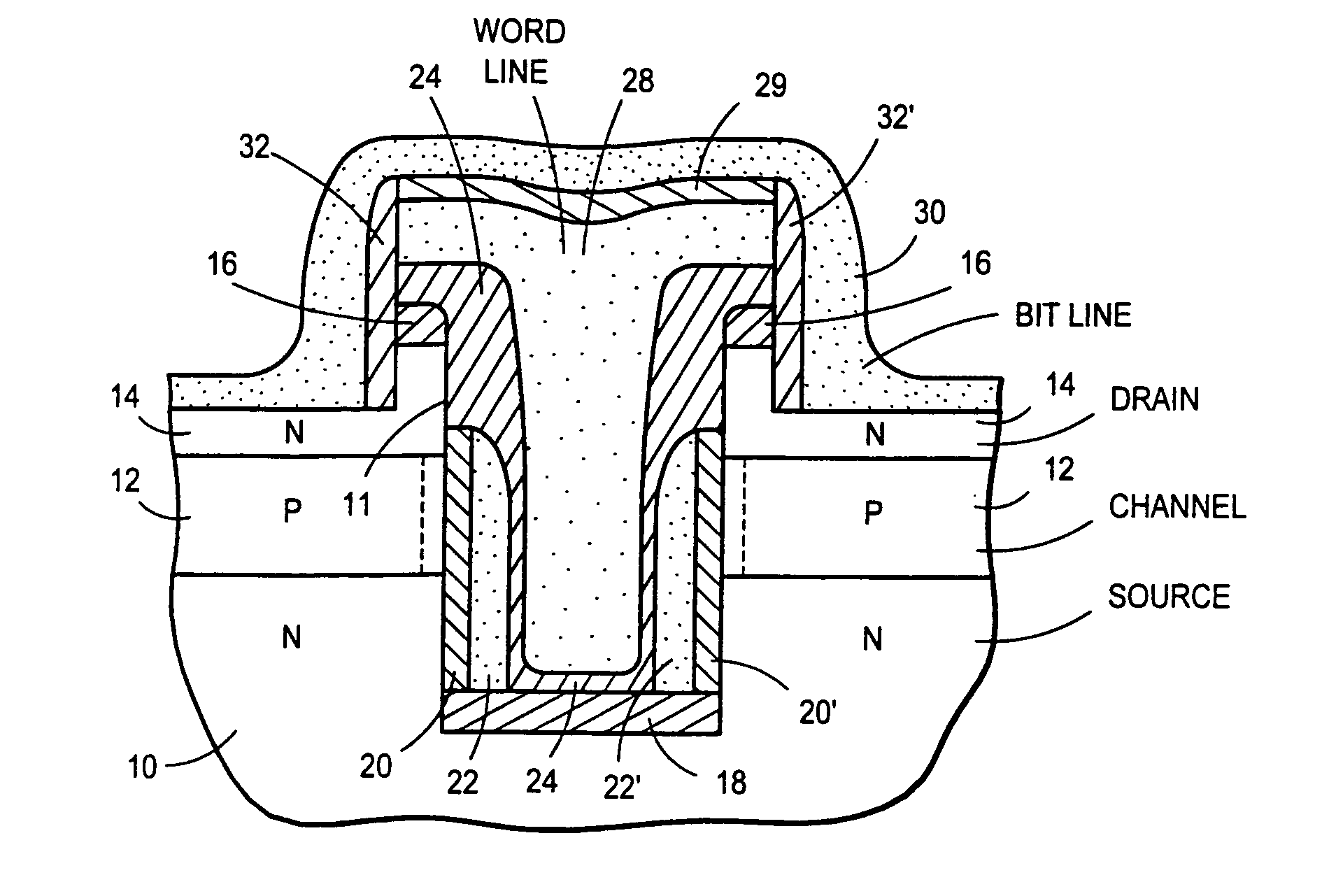
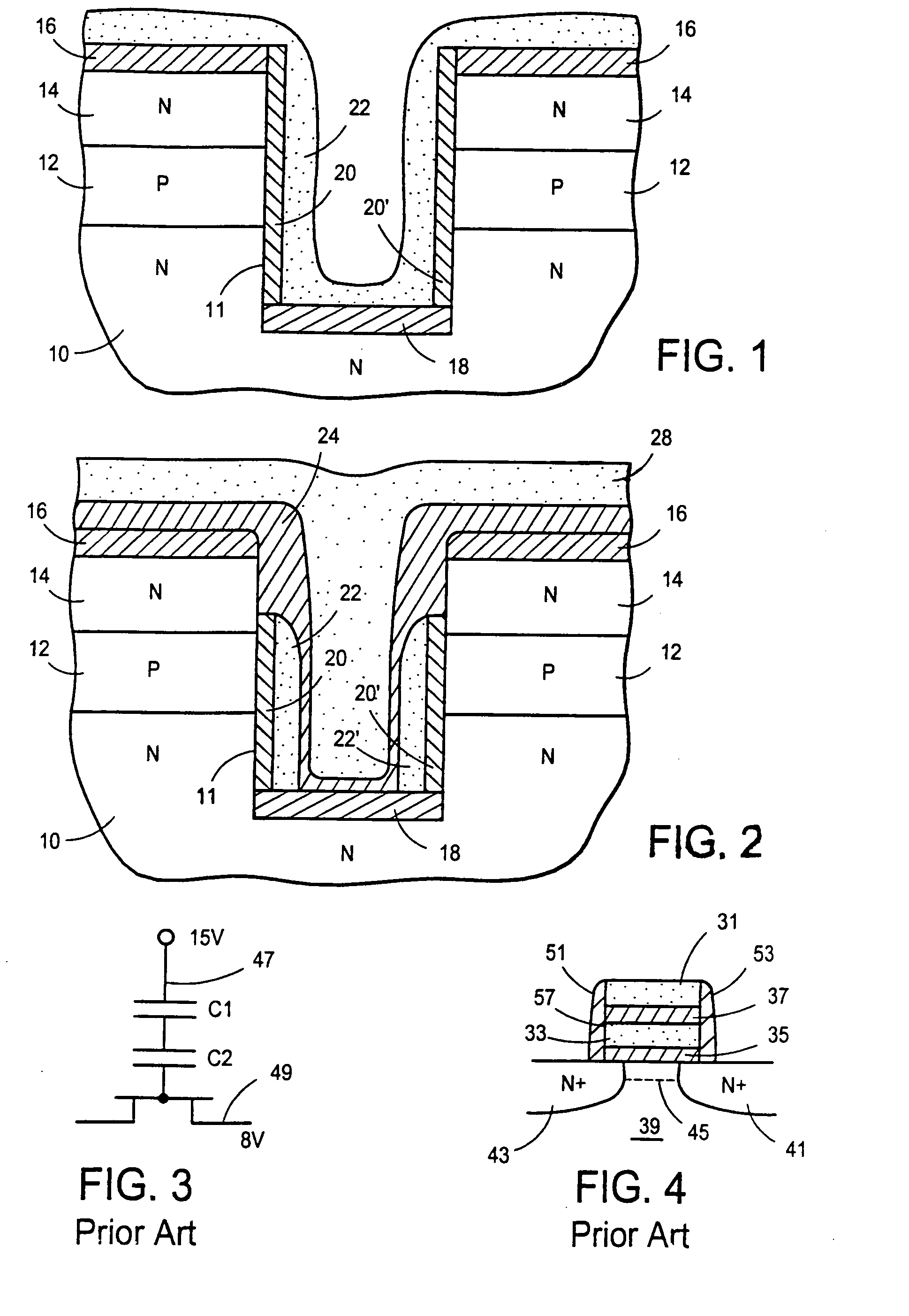
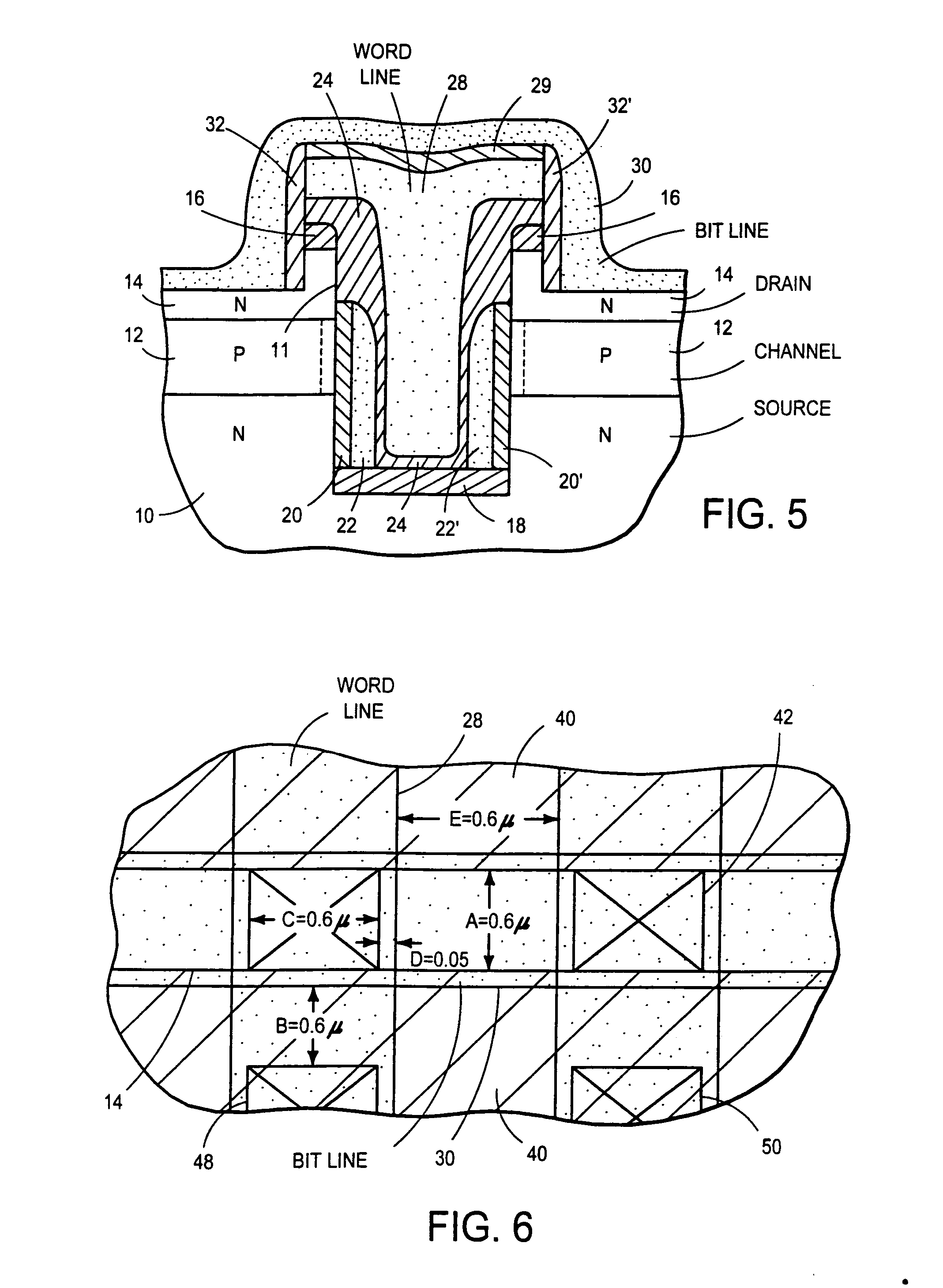
A nonvolative memory in the form of a vertifcal flash EPROM with high density and low cost. A vertical MOS transistor is formed in well etched into a semiconductor substrate, the substrate having source, body and drain regions formed by ion implantation. A thin gate oxide or oxide-nitride-oxide (ONO) layer is formed in the well and a self-aligned floating gate of polysilicon is formed over the gate oxide in the well to overlie the body region. An anisotropic etch is used to form the self aligned floating gate so as to remove all horizontal components and leave no portion of said floating gate extending beyond the perimeter of said well such that its lateral extents are determined by the anisotropic etch and not photolithography. Leff is determined by the energy of the implants used for form the source and drain regions and not by lithography. A deep field oxide bounding parts of said well keeps the coupling ratio good at all feature sizes. A vertically oriented NMOS and PMOS transistor are also disclosed.

Description


Claims


Application Information

Patent Timeline
Owner VORA MADHUKAR B
Learn More