MOSFET chip layout structure

A layout structure and chip technology, applied in electrical components, transistors, circuits, etc., can solve the problems of high chip on-resistance, insufficient chip performance, large chip area, etc., to improve chip performance, reduce chip cost, and reduce conduction. The effect of resistance

Active Publication Date: 2020-09-15
JIANGSU HAIDONG SEMICON TECH CO LTD
View PDF3 Cites 0 Cited by
  • Summary
  • Abstract
  • Description
  • Claims
  • Application Information

AI Technical Summary

Problems solved by technology

This leads to high on-resistance of the chip and insufficient chip performance; on the other hand, in order to achieve the target on-resistance, a larger chip area is required and the cost of the chip is higher

Method used


Image

  • MOSFET chip layout structure
  • MOSFET chip layout structure
  • MOSFET chip layout structure

Examples


Embodiment Construction

[0019] The present invention will be described in further detail below in conjunction with examples and specific implementation methods.

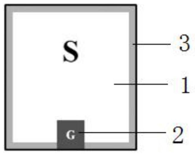
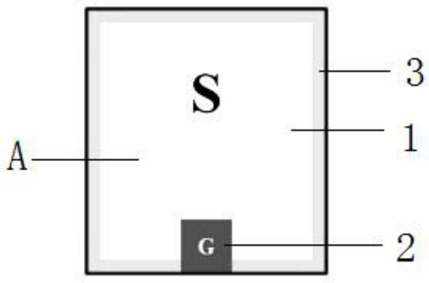
[0020] like image 3 As shown, a MOSFET chip layout structure is applied to a MOSFET chip, including the first layer of source metal at the bottom and the second layer of source metal in contact with the top surface of the first layer of source metal, the first layer of source metal The electrode metal is the source region 1 surrounded by the gate bus bar 3, the gate bus bar 3 has a gate etching window, the second layer of source metal covers the first layer of source metal, and the second layer of source metal A gate bonding region 2 is provided on the metal to be in contact with a gate bus bar 3 through a gate etching window.

[0021] The area of ​​the source metal of the second layer is larger than the area of ​​the source metal of the first layer.

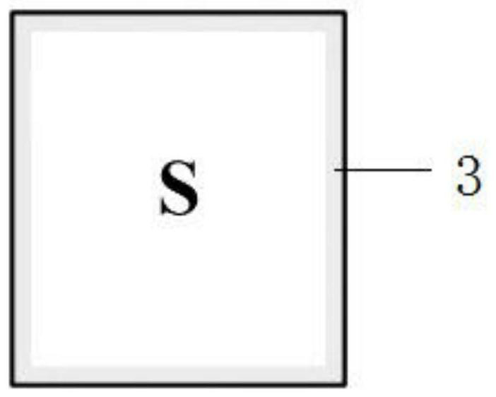
[0022] like figure 2 , 3 As shown, a method for manufacturing a MOSFET chip layout ...


PUM


Abstract

The invention relates to an MOSFET chip layout structure, which is applied to an MOSFET chip and comprises a first layer of source metal located at the bottom and a second layer of source metal makingcontact with the top surface of the first layer of source metal, wherein the first layer of source metal is a source region surrounded by a grid Bus bar, a grid etching window is formed in the grid Bus bar, the second layer of source metal covers the first layer of source metal, and a grid bonding region is arranged on the second layer of source metal and is in contact with the grid Bus bar through the grid etching window. The MOSFET chip layout structure has the advantages that the front metal adopts double-layer wiring, i.e., the first layer of metal is source metal except the grid Bus bar,so that the original grid bonding region can be completely expanded into a source region, the cellular region of the chip is increased, the on-resistance of the chip is effectively reduced, and the performance of the chip is improved; or under the condition of obtaining the same on-resistance, the area of the chip can be reduced, and finally the cost of the chip is reduced.

Description

technical field [0001] The invention relates to a MOSFET chip layout structure. Background technique [0002] Metal-Oxide Semiconductor Field-Effect Transistor, referred to as Metal-Oxide-Semiconductor Field-Effect Transistor, MOSFET, is a field-effect transistor that can be widely used in the field of power electronics. According to the polarity of its "channel" (working carrier), MOSFET can be divided into two types: "N-type" and "P-type", which are usually called NMOSFET and PMOSFET, and the abbreviation includes NMOS, PMOS, etc. [0003] The MOSFET chip in the prior art generally has a single-layer metal on the front side, and the two electrodes of the front side metal: the gate (G pole) and the source (S pole) can only be laid out on the same layer of metal, so the gate will occupy the source. part of the area of ​​the pole. like figure 1 As shown, the gate bonding area occupies more area of ​​the source area. As a result, the on-resistance of the chip is high and t...

Claims


Application Information

Patent Timeline
Patent Type & Authority Applications(China)
IPC IPC(8): H01L29/78H01L29/417H01L21/336
CPCH01L29/41758H01L29/66568H01L29/78
Inventor 夏华忠诸建周谈益民黄传伟李健其他发明人请求不公开姓名
Owner JIANGSU HAIDONG SEMICON TECH CO LTD
Why Eureka
Try Eureka