

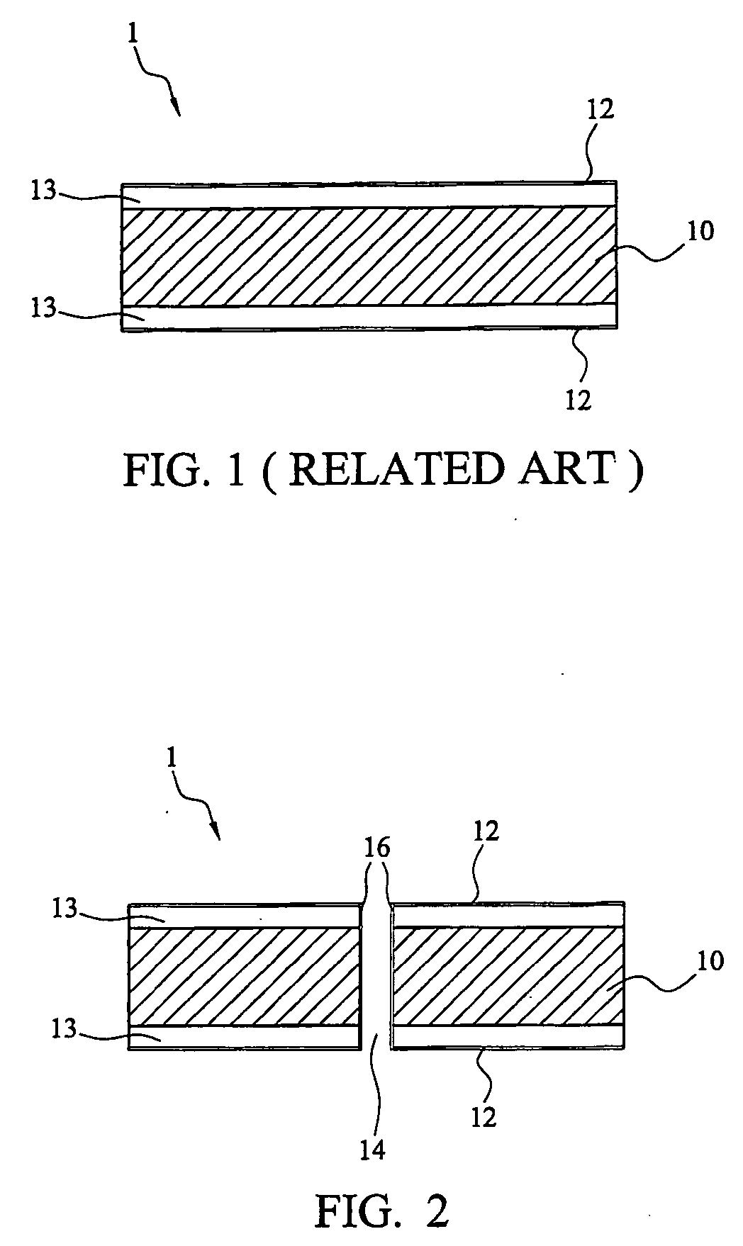
Circuit board with a through hole wire and manufacturing method thereof
a technology of circuit board and through hole wire, which is applied in the direction of printed circuit aspects, conductive pattern formation, electric connection formation of printed elements, etc., to achieve the effect of high heat dissipation capacity and high thermal conductivity of metal
- Summary
- Abstract
- Description
- Claims
- Application Information
AI Technical Summary
Benefits of technology
Problems solved by technology
Method used
Image

Examples
Embodiment Construction
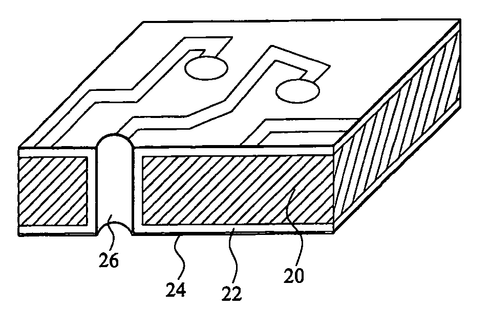
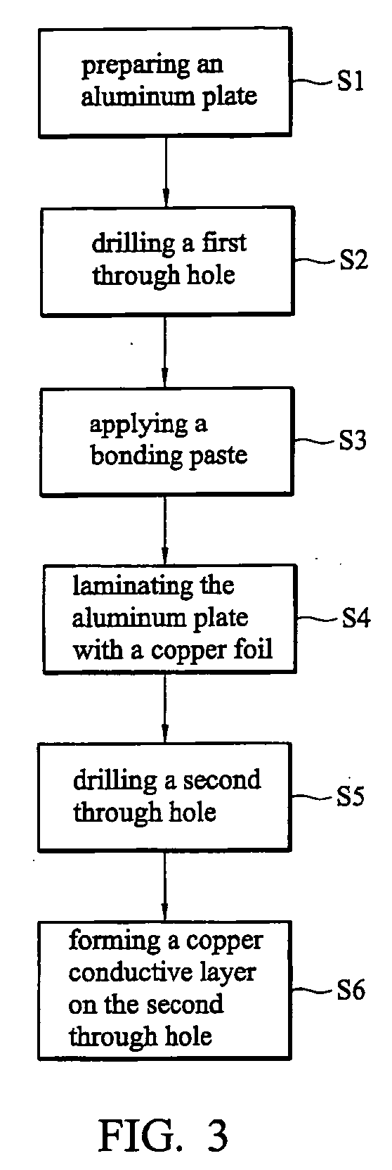
[0022] Referring to FIG. 3, FIG. 3 is a flowchart of an embodiment of a manufacturing method for a circuit board of SMD module.
[0023] In step S1, an aluminum substrate with a predetermined size is prepared.
[0024] In step S2, at least one first through hole is drilled in a predetermined position of the aluminum substrate.
[0025] In step S3, a binder is applied on upper and lower surfaces of the aluminum substrate.
[0026] In step S4, the upper and lower surfaces of the aluminum substrate are respectively laminated with copper foils so that the binder flows and the first through hole is filled with the binder; thereafter, the binder is solidified.
[0027] In step S5, by concentric with the first through hole, at least one second through hole is drilled at a predetermined size within the filled first through hole.
[0028] In step S6, a copper conductive layer is formed on an inner side wall of the second through hole by non-electrical plating and electrical plating.
[0029] In steps S2 a...
PUM
| Property | Measurement | Unit |
|---|---|---|
| Time | aaaaa | aaaaa |
| Pressure | aaaaa | aaaaa |
| Electrical conductor | aaaaa | aaaaa |
Abstract
Description
Claims
Application Information