Flash memory device with improved management of protection information
- Summary
- Abstract
- Description
- Claims
- Application Information
AI Technical Summary
Benefits of technology
Problems solved by technology
Method used
Image


Examples
Embodiment Construction
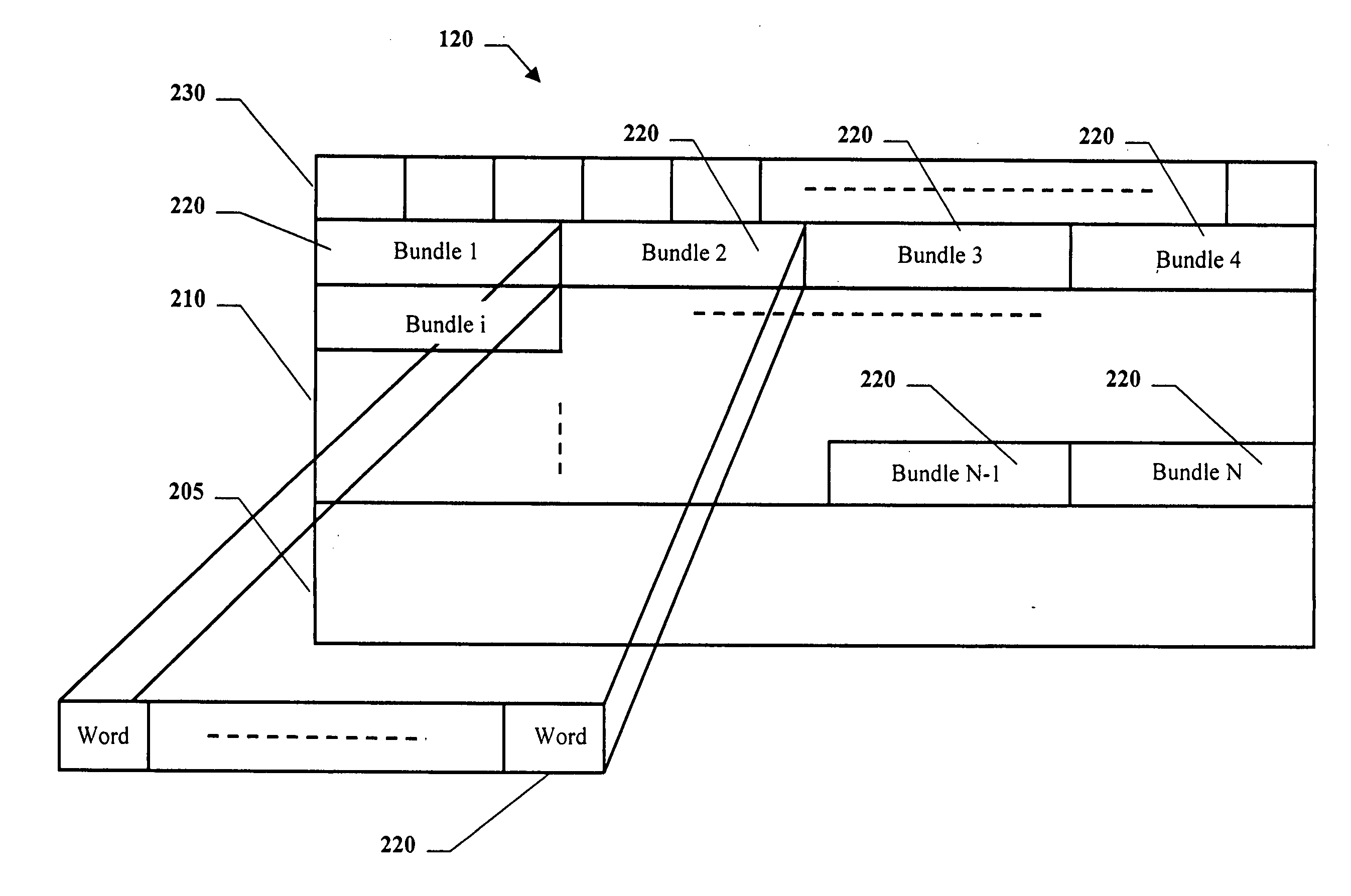
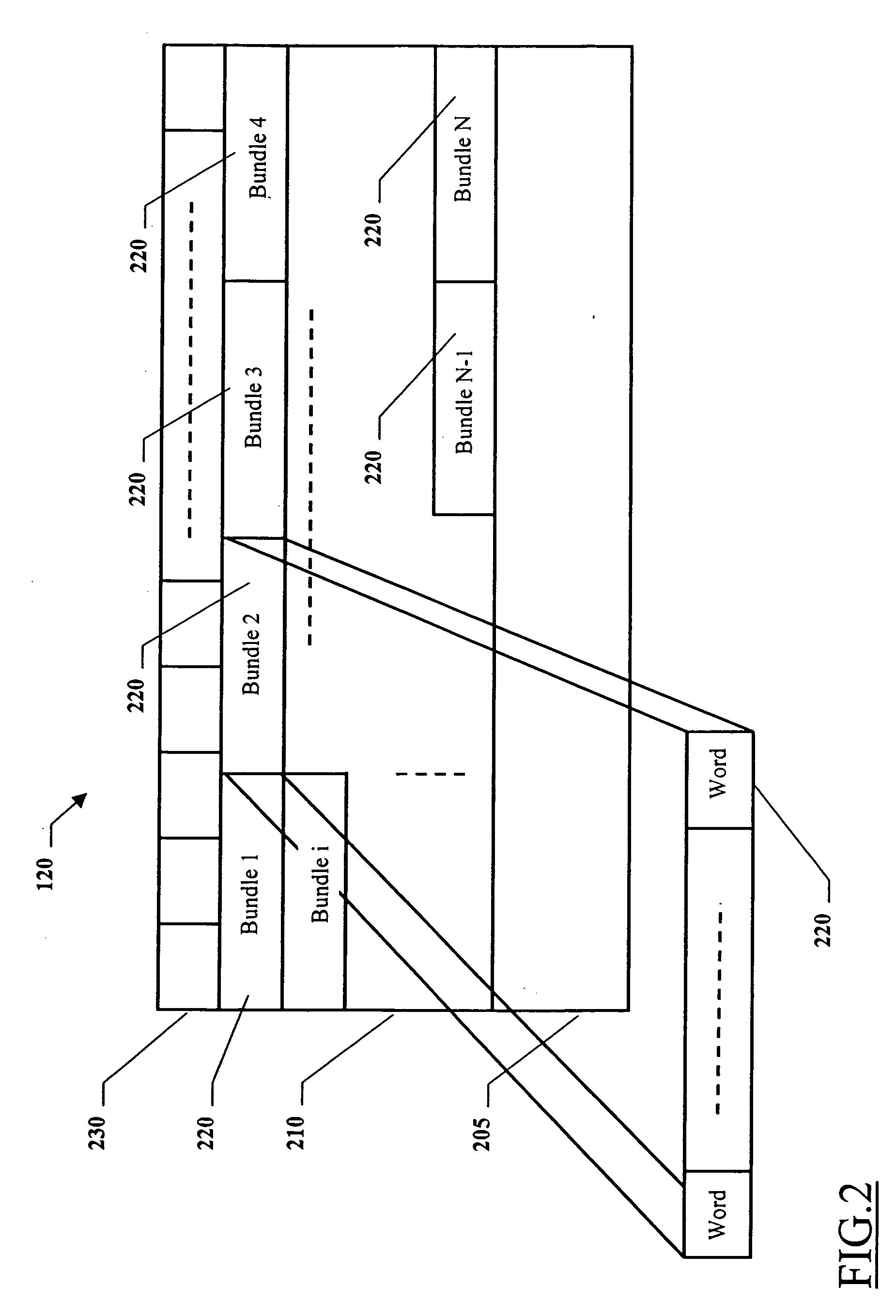
[0031] Referring in particular to FIG. 1, a non-volatile memory device of flash type 100 is shown. The memory device 100 includes a matrix 110 of cells that are typically floating gate MOS transistors although other transistor types may be used; the matrix 110 is partitioned in several sectors 120 (for example, 16), each one being individually erasable. Typically, each cell stores the logical value “1” when it is erased and the logical value “0” when it is programmed.
[0032] The memory device 100 receives an address ADD from the outside. A portion of the address is provided to a row decoder 130 and another portion of the address ADD is provided to a column decoder 140; the decoders 130, 140 select a block of memory cells (for example, 8), which store a word (8 bits in the case at issue) being processed in parallel.
[0033] The column decoder 140 interfaces with read / write circuits 150, which include all components (for example, sense amplifiers, comparators and similar circuits) that...
PUM
 Abstract
Description
Claims
Application Information
 - R&D Engineer
- R&D Manager
- IP Professional
- Industry Leading Data Capabilities
- Powerful AI technology
- Patent DNA Extraction
Browse by: Latest US Patents, China's latest patents, Technical Efficacy Thesaurus, Application Domain, Technology Topic.
© 2024 PatSnap. All rights reserved.Legal|Privacy policy|Modern Slavery Act Transparency Statement|Sitemap