STRUCTURE AND METHOD FOR IMPROVED STRESS AND YIELD IN pFETS WITH EMBEDDED SiGe SOURCE/DRAIN REGIONS

a technology of source/drain region and structure, which is applied in the direction of basic electric elements, electrical apparatus, semiconductor devices, etc., can solve the problems of difficult contact with the device, significant impediments, and silicide shorting of the source/drain to the body, and achieves a higher uniaxial stress

Active Publication Date: 2007-01-25
GLOBALFOUNDRIES US INC
View PDF4 Cites 119 Cited by
  • Summary
  • Abstract
  • Description
  • Claims
  • Application Information

AI Technical Summary

Benefits of technology

[0012] The present invention provides a technique for forming a CMOS structure including at least one pFET that has a stressed channel which avoids the problems mentioned in the prior art. That is, the present invention provides a method for avoiding the formation of deep canyons at the interface between the active area and the trench isolation region, without requiring a trench isolation pulldown, thereby eliminating the problems of silicide to source / drain shorts and contact issues. At the same time, the method of the present invention provides a structure that allows for a facet to form at the spacer edge, retaining the Miller capacitance benefit that such a structure provides. The inventive structure also results in higher uniaxial stress in the MOSFET channel compared to one which allows for a facet to grow at the trench isolation edge.

Problems solved by technology

This same tendency occurs on shallow trench isolation (STI) sidewalls as well, creating deep canyons which can cause significant impediments to the successful integration of embedded SiGe devices to an existing device flow.
Some issues that need to be addressed in prior art embedded SiGe devices include the potential silicide shorting of the source / drain to the body in bulk semiconductors, a difficulty in contacting the device due to inadequate clearing of the middle-of-the-line (MOL) dielectric and the contact etch stop liner in the canyon (which are critical for both bulk and semiconductor-on-insulator (SOI) technologies).
Further, faceted growth at the STI sidewall results in a reduction of stress in the channel, which is particularly problematic in devices with relatively small gate to STI distance.
In doing so, the issue of contacting the device is alleviated, but the risk of silicide shorts between the source / drain and the body remain, and due to the STI pulldown, both the nFET and the pFET become vulnerable to this problem.
The existence of spacers on the STI sidewalls would result in incomplete silicidation of the source and drain and is expected to negatively impact manufacturing yield.

Method used


Image

  • STRUCTURE AND METHOD FOR IMPROVED STRESS AND YIELD IN pFETS WITH EMBEDDED SiGe SOURCE/DRAIN REGIONS
  • STRUCTURE AND METHOD FOR IMPROVED STRESS AND YIELD IN pFETS WITH EMBEDDED SiGe SOURCE/DRAIN REGIONS
  • STRUCTURE AND METHOD FOR IMPROVED STRESS AND YIELD IN pFETS WITH EMBEDDED SiGe SOURCE/DRAIN REGIONS

Examples


Embodiment Construction

[0030] The present invention, which provides a structure and a method for improved stress and yield in a CMOS technology including at least one pFET, will be described in greater detail by referring to the following discussion, together with the drawings that accompany the present application. It is noted that the drawings of the present invention are provided for illustrative purposes and thus they are not drawn to scale.

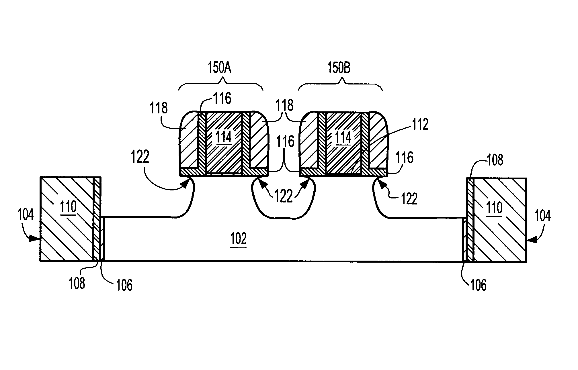
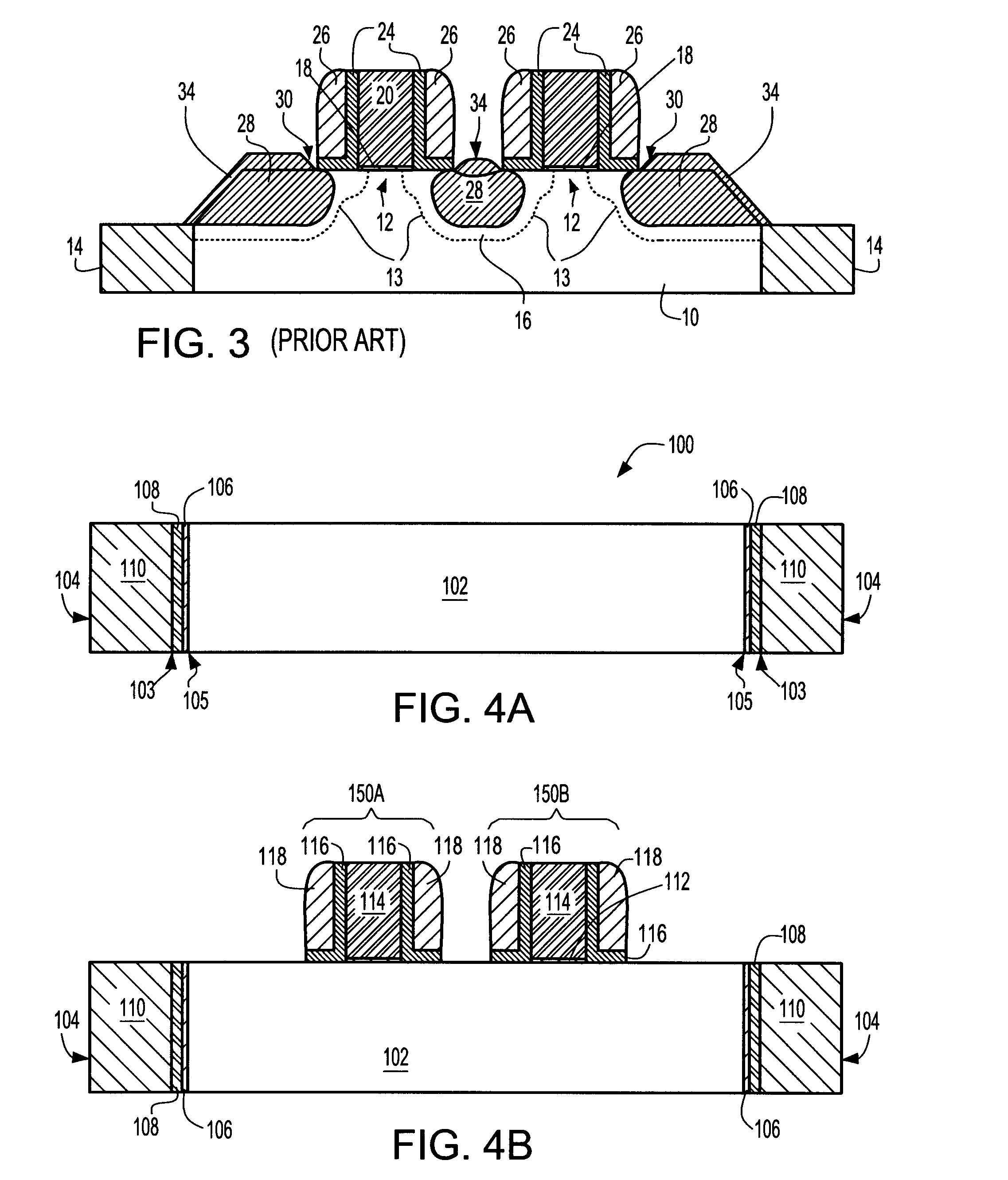
[0031] Reference is first made to the initial structure 100 shown in FIG. 4A. Specifically, structure 100 includes a semiconductor substrate 102 that has at least one trench isolation region 104 embedded within the substrate. As shown, the at least one trench isolation region 104 comprises an oxide liner 106 which is in contact with the semiconductor substrate 102 and lining walls of a trench located within the semiconductor substrate 102. The at least one trench isolation region 104 also includes a nitride liner 108 on the oxide liner 106 and a trench dielectric ...


PUM


Abstract

The present invention provides a technique for forming a CMOS structure including at least one pFET that has a stressed channel which avoids the problems mentioned in the prior art. Specifically, the present invention provides a method for avoiding formation of deep canyons at the interface between the active area and the trench isolation region, without requiring a trench isolation pulldown, thereby eliminating the problems of silicide to source/drain shorts and contact issues. At the same time, the method of the present invention provides a structure that allows for a facet to form at the spacer edge, retaining the Miller capacitance benefit that such a structure provides. The inventive structure also results in higher uniaxial stress in the MOSFET channel compared to one which allows for a facet to grow at the trench isolation edge.

Description

FIELD OF THE INVENTION [0001] The present invention relates to a strained semiconductor structure and a method of forming the same. More particularly, the present invention relates to a strained complementary metal oxide semiconductor (CMOS) structure in which the stress in the channel region is enhanced. The present invention also provides a method of fabricating the CMOS structure of the present invention in which the process yield is improved compared to prior art techniques. BACKGROUND OF THE INVENTION [0002] In present semiconductor technology, CMOS devices, such as nFETs or pFETs, are typically fabricated upon semiconductor wafers, such as Si, that have a single crystal orientation. In particular, most of today's semiconductor devices are built upon Si having a (100) crystal orientation. [0003] Stress can be introduced into a single crystal oriented substrate by several methods including, for example, forming a stress inducing liner on top of the substrate and around the gate ...

Claims


Application Information

Patent Timeline
Patent Type & Authority Applications(United States)
IPC IPC(8): H01L29/78H01L21/336
CPCH01L21/823412H01L21/823425H01L21/823807H01L29/7848H01L29/165H01L29/66628H01L29/66636H01L21/823814H01L29/665
Inventor CHIDAMBARRAO, DURESETIGREENE, BRIAN J.
Owner GLOBALFOUNDRIES US INC
Why Eureka
Try Eureka