Electron emission device, electron emission type backlight unit and flat display apparatus having the same

Inactive Publication Date: 2007-01-25
SAMSUNG SDI CO LTD
View PDF42 Cites 24 Cited by
  • Summary
  • Abstract
  • Description
  • Claims
  • Application Information

AI Technical Summary

Benefits of technology

[0017] Aspects of the present invention provide an electron emission device and an electron emission type backlight unit having a new structure using the electron emission device in which an electric field between an

Problems solved by technology

In addition, due to the light-emitting characteristic of phosphor materials, during a predetermined period of time in which light is emitted by electrons that are incident on a phosphor material, other incident electrons cannot contribute to light emission.
Thus light-emitting efficiency is not improved by incr

Method used


Image

  • Electron emission device, electron emission type backlight unit and flat display apparatus having the same
  • Electron emission device, electron emission type backlight unit and flat display apparatus having the same
  • Electron emission device, electron emission type backlight unit and flat display apparatus having the same

Examples


Embodiment Construction

[0041] Reference will now be made in detail to the present embodiments of the present invention, examples of which are illustrated in the accompanying drawings, wherein like reference numerals refer to the like elements throughout. The embodiments are described below in order to explain the present invention by referring to the figures.

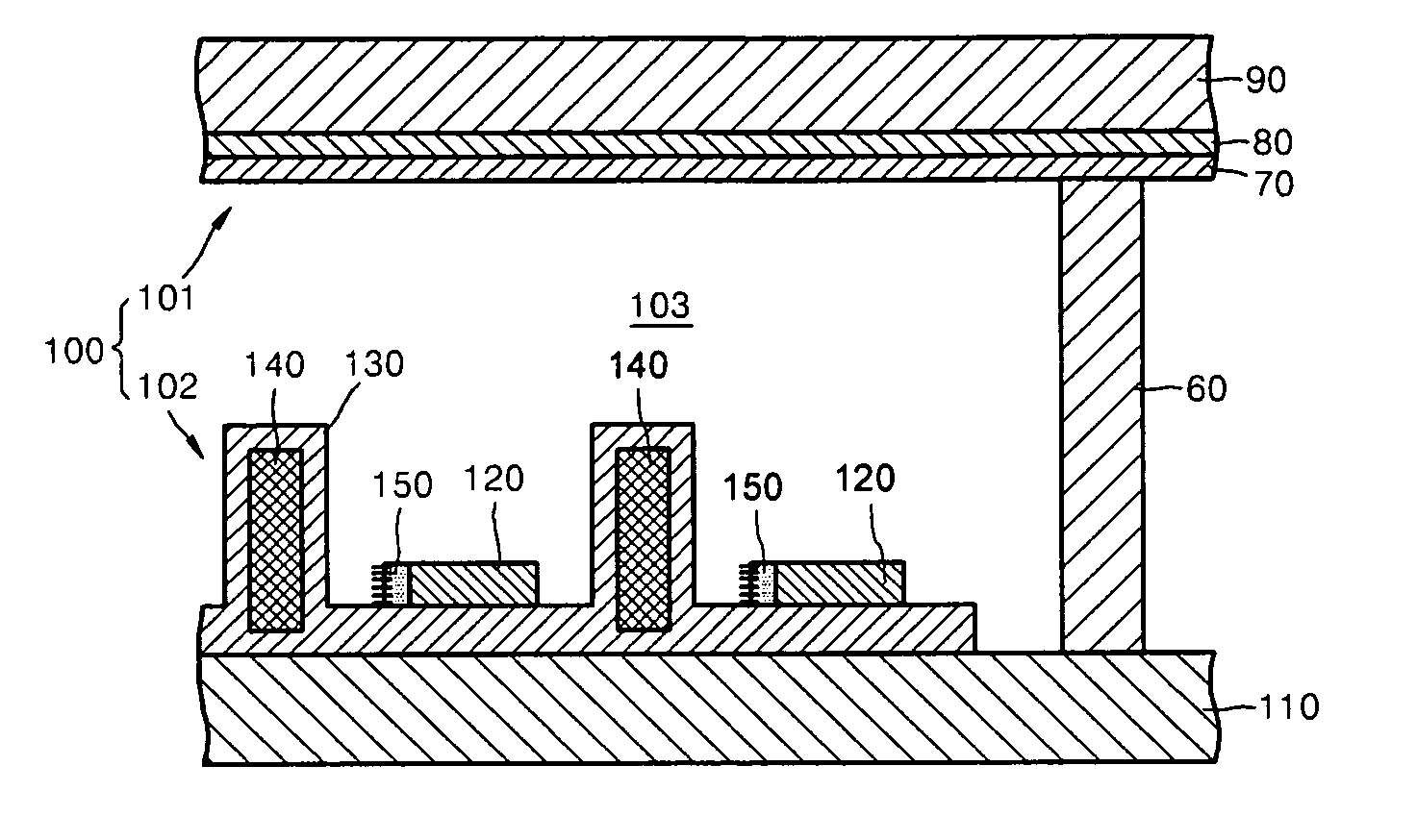
[0042]FIG. 2 is a cross-sectional view of an electron emission type backlight unit 100 and an electron emission device 102 according to an embodiment of the present invention.

[0043] Referring to FIG. 2, the electron emission type backlight unit 100 includes a front panel 101 and the electron emission device 102 that are separated from and parallel to each other. A vacuum space 103 is formed between the front panel 101 and the electron emission device 102, and a spacer 60 maintains a distance between the front panel 101 and the electron emission device 102.

[0044] The front panel 101 includes a front substrate 90, an anode electrode 80 disposed on a ...


PUM


Abstract

An electron emission device having improved electron emission efficiency and an electron emission type backlight unit including the electron emission device in which an electric field between an anode electrode and a cathode electrode is effectively blocked, and electrons are emitted continuously and stably by a low gate voltage, thereby improving light-emitting uniformity and light-emitting efficiency. Also provided is a flat display apparatus employing the electron emission type backlight unit having the electron emission device. The electron emission device includes a base substrate; an insulating layer disposed on a surface of the base substrate; a cathode electrode formed on the insulating layer; a gate electrode that is formed on the base substrate, separated from the cathode electrode, and higher than the cathode electrode; and an electron emission layer that is electrically connected to the cathode electrode and disposed to face the gate electrode.

Description

CROSS-REFERENCE TO RELATED APPLICATIONS [0001] This application claims the benefit of Korean Application No. 2005-66380, filed Jul. 21, 2005, in the Korean Intellectual Property Office, the disclosure of which is incorporated herein by reference. BACKGROUND OF THE INVENTION [0002] 1. Field of the Invention [0003] Aspects of the present invention relate to an electron emission device, an electron emission type backlight unit, and a flat display apparatus having the same, and more particularly, to an electron emission device with improved electron emission efficiency and light-emitting uniformity, an electron emission type backlight unit employing the electron emission device, and a flat display apparatus having the electron emission type backlight unit. [0004] 2. Description of the Related Art [0005] Generally electron emission devices can be classified into electron emission devices using a thermionic cathode and electron emission devices using a cold cathode as an electron emission...

Claims


Application Information

Patent Timeline
IPC IPC(8): H01J1/00H01J9/02H01J19/06
CPCH01J63/06H01J61/305H01J1/30
Inventor CHO, YOUNG-SUKBAE, JAE-WOOKANG, DONG-HYUNLIM, IK-CHULDO, UI-SONGJOO, KYU-NAM
Owner SAMSUNG SDI CO LTD
Why Eureka
Try Eureka