Electron-emitting device provided with pores that have carbon deposited therein

a carbon-deposited, electron-emitting technology, applied in the manufacture of electrode systems, discharge tubes with luminescent screens, discharge tubes, etc., can solve the problems of poor repeatability, impede the enhancement of definition, and spread of electron beams

Inactive Publication Date: 2002-10-29
CANON KK
View PDF14 Cites 99 Cited by
  • Summary
  • Abstract
  • Description
  • Claims
  • Application Information

AI Technical Summary

Problems solved by technology

According to the studies by Spindt et al., the conventional FE type electron-emitting devices, however, had a problem of a spread of the electron beam, which was hindrance against enhancement of definition.
In the example of application of the holes of the anodic oxide film to the apertures of the gate electrode, there remained a problem of poor repeatability in formation of the cone of the electron-emitting region.
In the example in which the electron-emitting regions were formed in the cylindrical shape, there also arose problems of poor repeatability of the electron emission characteristics and high driving voltage.
In the surface conduction electron-emitting device provided with the correcting electrode, the electron emission efficiency was increased, but the potential of the correcting electrode was high, which was a problem in driving.
In an electron source equipped with many devices, variations in the thickness of the insulating layer are directly bound to variations in the emission current, so that control of variations is difficult.
When an image pickup device or an image forming device is constructed using the electron source; there will arise a problem of degradation of image quality.
Second, the quality of the insulating layer did not affect only the electron emission characteristics, but also affected the device current.
Particularly, in the case of a large area, control of variations is difficult.
In the image pickup device or the image forming device using the electron source, there will arise the problem of degradation of image quality.
Third, repeatability was poor as to occurrence of the negative resistance and occurrence of the fluctuation of the device current and control thereof was difficult.
In the conventional surface conduction electron-emitting device provided with the correcting electrode, the electron emission efficiency was increased, but the potential of the correcting electrode was high, which was the problem in driving.

Method used


Image

  • Electron-emitting device provided with pores that have carbon deposited therein
  • Electron-emitting device provided with pores that have carbon deposited therein
  • Electron-emitting device provided with pores that have carbon deposited therein

Examples


first embodiment

of the First Embodiment

FIG. 7A is a plan view of a substrate on which five electron-emitting devices of the present invention are placed and FIG. 7B is a schematic sectional view along 7B-7B of FIG. 7A.

In FIGS. 7A and 7B, numeral 1 denotes a substrate, 73 anodic oxide layers, 71 lead wires of the lower electrodes, 72 a lead wire of the upper electrodes, and 74 intersections between the lead wires 71 of the lower electrodes and the lead wire 72 of the upper electrodes, at which the electron-emitting devices of the present invention are placed.

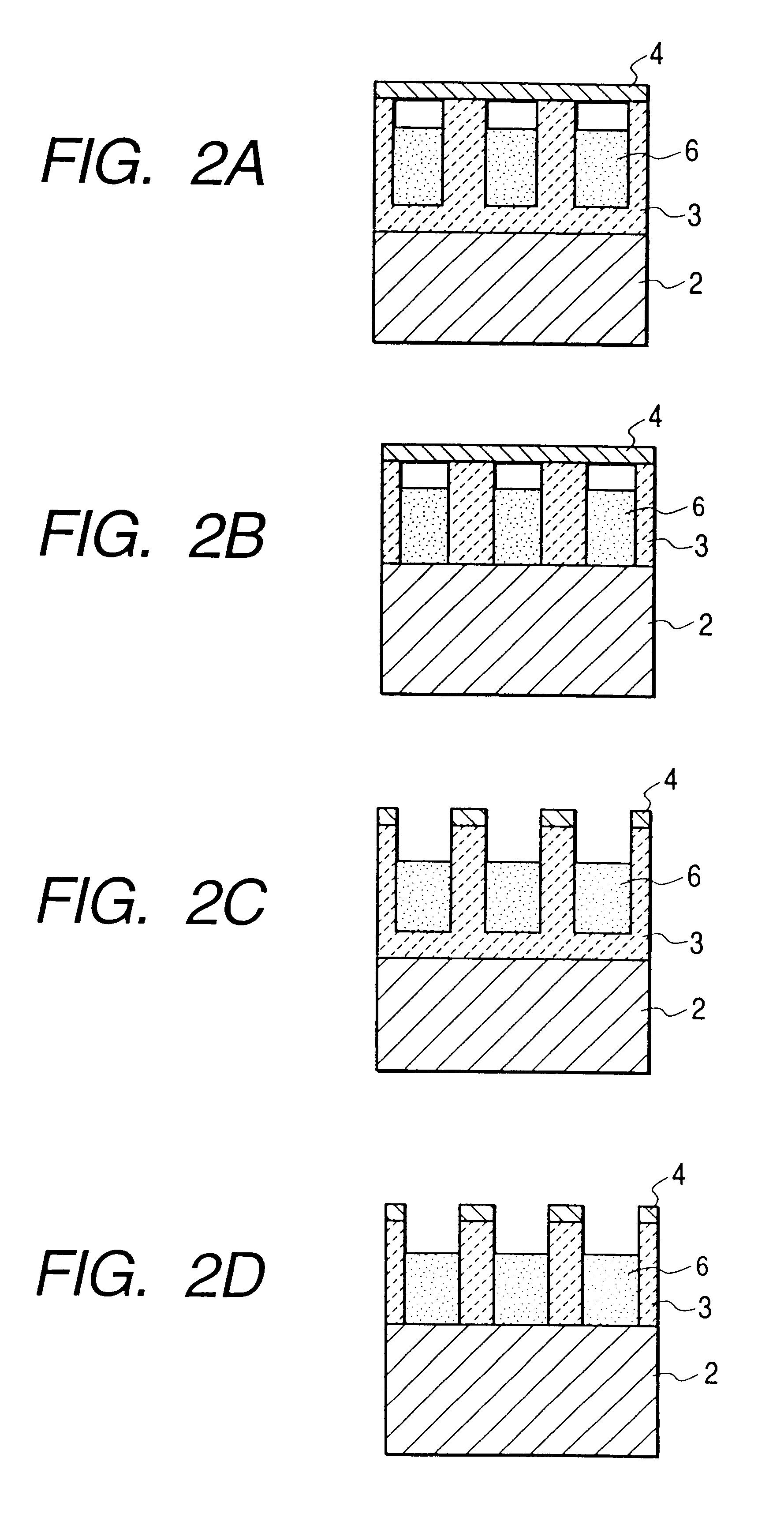
In the present example, substrates, each including five electron-emitting devices in either one of the structures of the four types illustrated in FIGS. 2A, 2B, 2C, and 2D, will be called substrates A, B, C, and D, respectively.

A production method of the present example will be described specifically.

(Step 1: Step of Forming the Lower Electrode of Metal on the Substrate)

The substrate 1 of quartz glass was washed well with detergent, pure water, ...

second embodiment

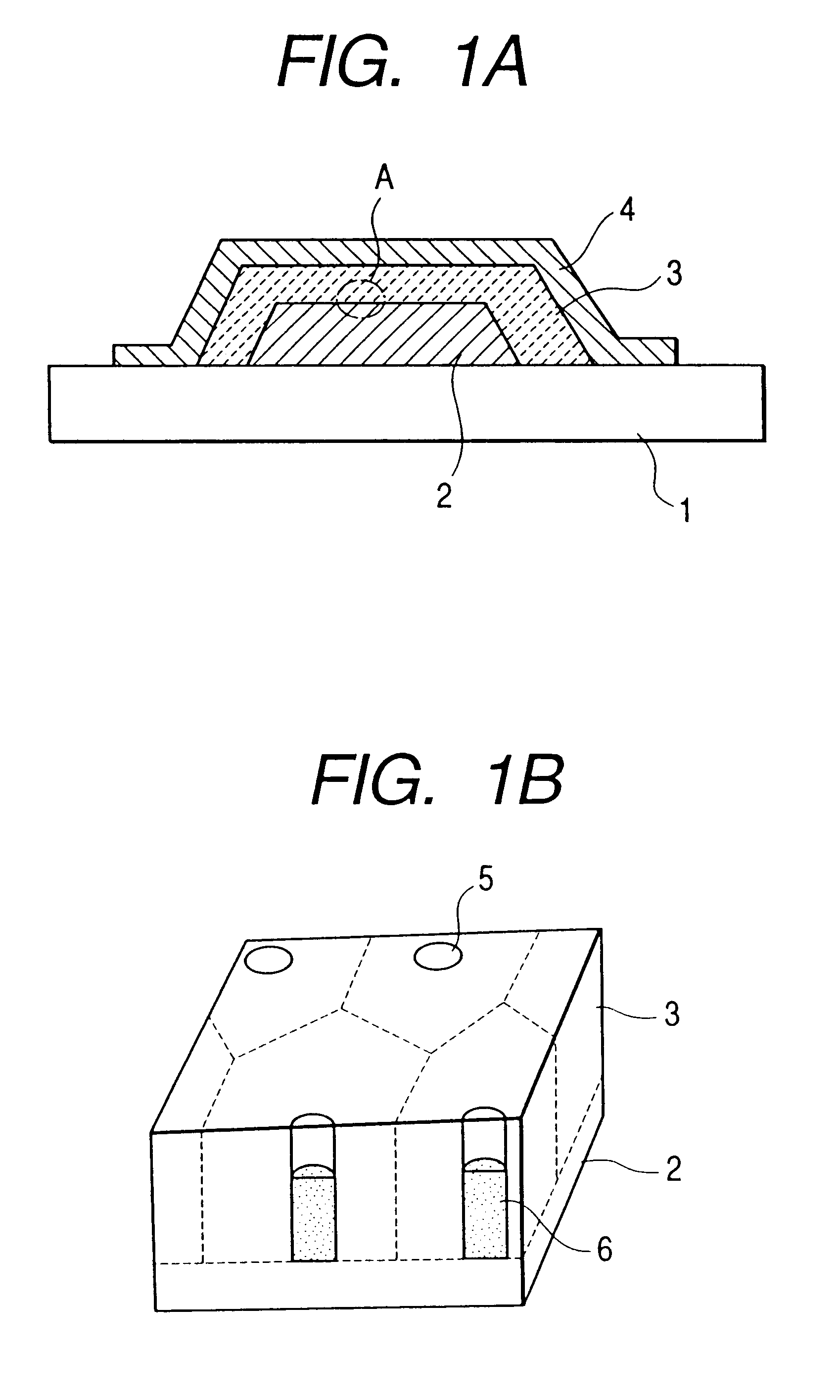
FIG. 11A is a sectional view of the second embodiment. FIG. 11B is a partly enlarged, schematic view of part A in the sectional view of FIG. 11A. The present embodiment uses the anodic oxide layer for the insulating layer. In FIG. 11A reference numerals are given in the similar fashion to those in FIGS. 1A and 1B.

The substrate 1 to be employed herein can be selected from quartz glass, glass with a decreased content of impurity such as Na, soda lime glass, a glass substrate obtained by depositing SiO.sub.2 on soda lime glass by sputtering or the like, ceramics such as alumina, an Si substrate, an Si substrate with a deposited layer of SiO.sub.2, and so on. Particularly, when the substrate 1 is a semiconductor substrate, a driver or the like for driving the electron-emitting device can also be mounted simultaneously.

The lower electrode 2 is selected from metals, such as Al, Ta, Nb, Ti, Zr, Hf, or Si, and semiconductors that can undergo anodic oxidation. The thickness of the lower elec...

third embodiment

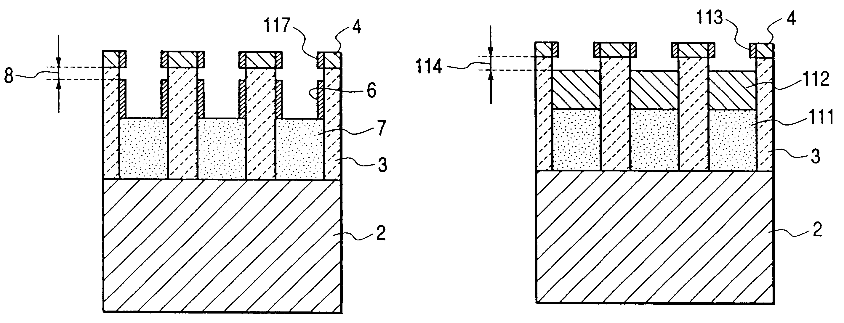
FIG. 20A is a sectional view of the electron-emitting device of the present embodiment. FIG. 20B is a partly enlarged, schematic view of part A in the sectional view of FIG. 20A. The present embodiment is application of the anodic oxide layer to the insulating layer. FIGS. 21A to 21D illustrate respective electron-emitting devices having a variety of electron-emitting bodies. FIGS. 22A and 22B show other structural examples.

In FIGS. 20A and 20B and FIGS. 21A to 21D, numeral 1 denotes a substrate, 2 an upper electrode, 3 an anodic oxide layer, 4 an upper electrode, 5 pores of the porous structure, 6 electron-emitting bodies, and 207 a small gap.

The substrate 1 to be employed herein can be selected from quartz glass, glass with a decreased content of impurity such as Na, soda lime glass, a glass substrate obtained by depositing SiO.sub.2 on soda lime glass by sputtering or the like, ceramics such as alumina, an Si substrate, an Si substrate with a deposited layer of SiO.sub.2, and so ...


PUM


Abstract

An electron-emitting device disclosed has stable electron emission characteristics with little variation, in high electron emission efficiency, in high definition, and at low driving voltage. The electron-emitting device disclosed is constructed in such structure that on a substrate there are a lower electrode, an insulating layer having pores, and an upper electrode stacked in this order, the insulating layer is an anodic oxide layer, and a carbon deposit is formed in the pores.

Description

1. Field of the InventionThe present invention relates to an electron-emitting device and a production method thereof and, more particularly, to an electron-emitting device having a lower electrode, an insulating layer having pores, and an upper electrode stacked in this order on a substrate, and a method for producing the electron-emitting device.2. Related Background ArtThe conventionally known electron-emitting devices are generally classified under two kinds, thermionic emission devices and cold cathode emission devices. The cold cathode emission devices include field emission type (FE type) devices, metal / insulator / metal type (MIN type) devices, surface conduction electron-emitting devices, and so on.The FE type devices are disclosed, for example, in W. P. Dyke & W. W. Dolan, "Field emission," Advance in Electron Physics, 8, 89 (1956) or in C. A. Spindt, "PHYSICAL Properties of thin-film field emission cathodes with molybdenum cones," J. Appl. Phys., 47, 5248 (1976).The tip of ...

Claims


Application Information

Patent Timeline
Patent Type & Authority Patents(United States)
IPC IPC(8): H01J9/02H01J1/30H01J1/304H01J1/312H01J1/316H01J29/04H01J31/12H01J31/38
CPCH01J1/30H01J9/022
Inventor YAMANOBE, MASATOTSUKAMOTO, TAKEOKAWATE, SHINICHI
Owner CANON KK
Why Eureka
Try Eureka