Light-Emitting Element, Light-Emitting Device, Display Device, Electronic Appliance, and Lighting Device

a technology of light-emitting elements and display devices, which is applied in the direction of semiconductor devices, solid-state devices, thermoelectric devices, etc., can solve the problems of affecting the practical application of light-emitting elements, and achieve favorable emission efficiency, low cost, and favorable emission efficiency

Active Publication Date: 2014-02-06
SEMICON ENERGY LAB CO LTD
View PDF1 Cites 91 Cited by
  • Summary
  • Abstract
  • Description
  • Claims
  • Application Information

AI Technical Summary

Benefits of technology

[0049]According to another embodiment of the present invention, a multicolor light-emitting element using fluorescence and phosphorescence, which has favorable emission efficiency, can be provided.
[0050]According to another embodiment of the present invention, a multicolor light-emitting element using fluorescence and phosphorescence, which has a relatively small number of layers to be formed, is advantageous for practical application, and has favorable emission efficiency, can be provided.
[0051]According to another embodiment of the present invention, a light-emitting device, a display device, an electronic appliance, and a lighting device each of which can be manufactured at low cost by using any of the above-described light-emitting elements can be provided.
[0052]According to another embodiment of the present invention, a light-emitting device, a display device, an electronic appliance, and a lighting device each of which has reduced power consumption by using any of the above-described light-emitting elements can be provided.

Problems solved by technology

The multicolor light-emitting element having the above-described structure in which the reliability is put ahead of the performance is suitable for practical application; on the other hand, a larger number of films are formed in order to obtain one light-emitting element, which hinders the practical application of the light-emitting element.

Method used


Image

  • Light-Emitting Element, Light-Emitting Device, Display Device, Electronic Appliance, and Lighting Device
  • Light-Emitting Element, Light-Emitting Device, Display Device, Electronic Appliance, and Lighting Device
  • Light-Emitting Element, Light-Emitting Device, Display Device, Electronic Appliance, and Lighting Device

Examples


embodiment 1

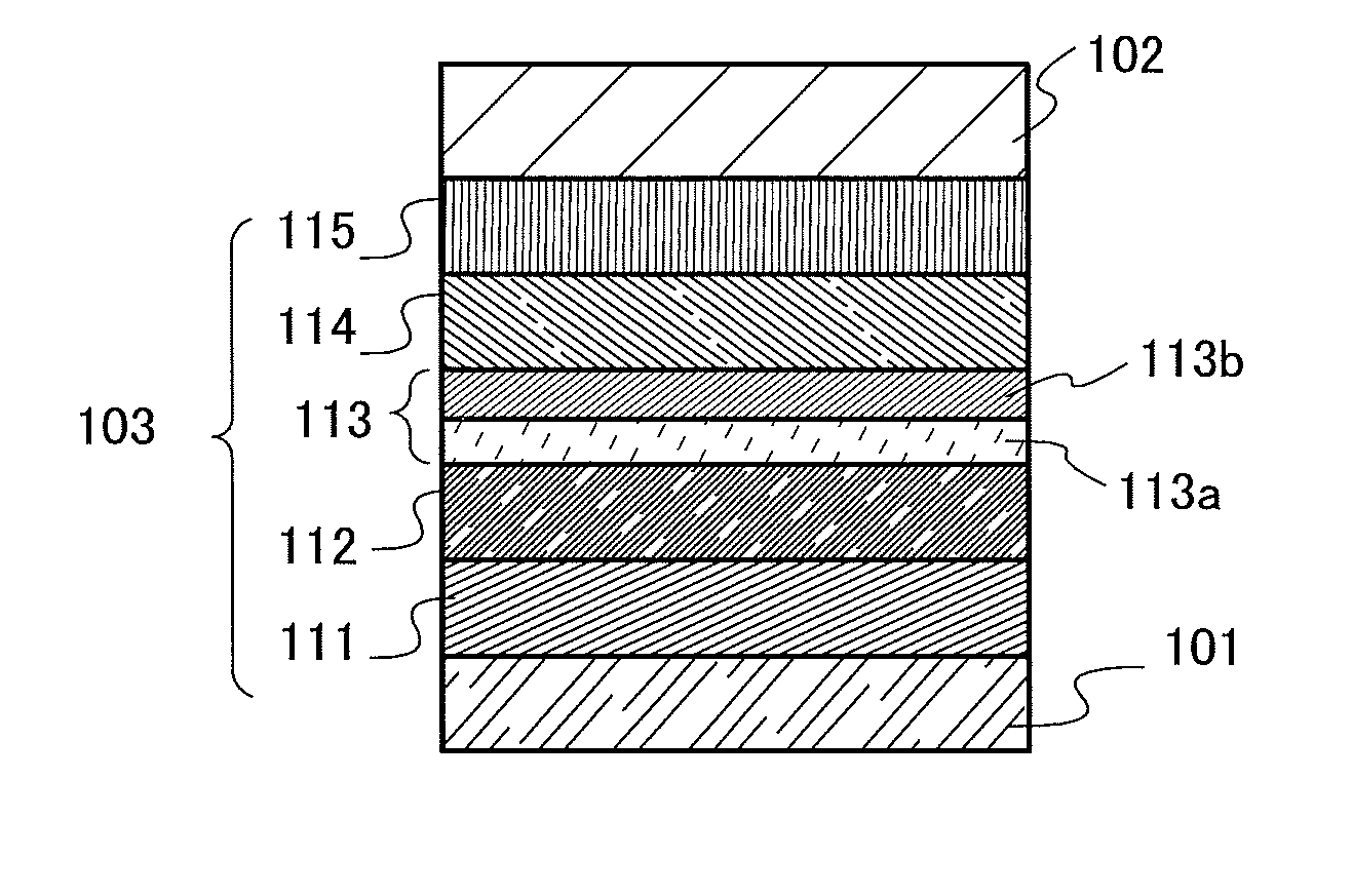
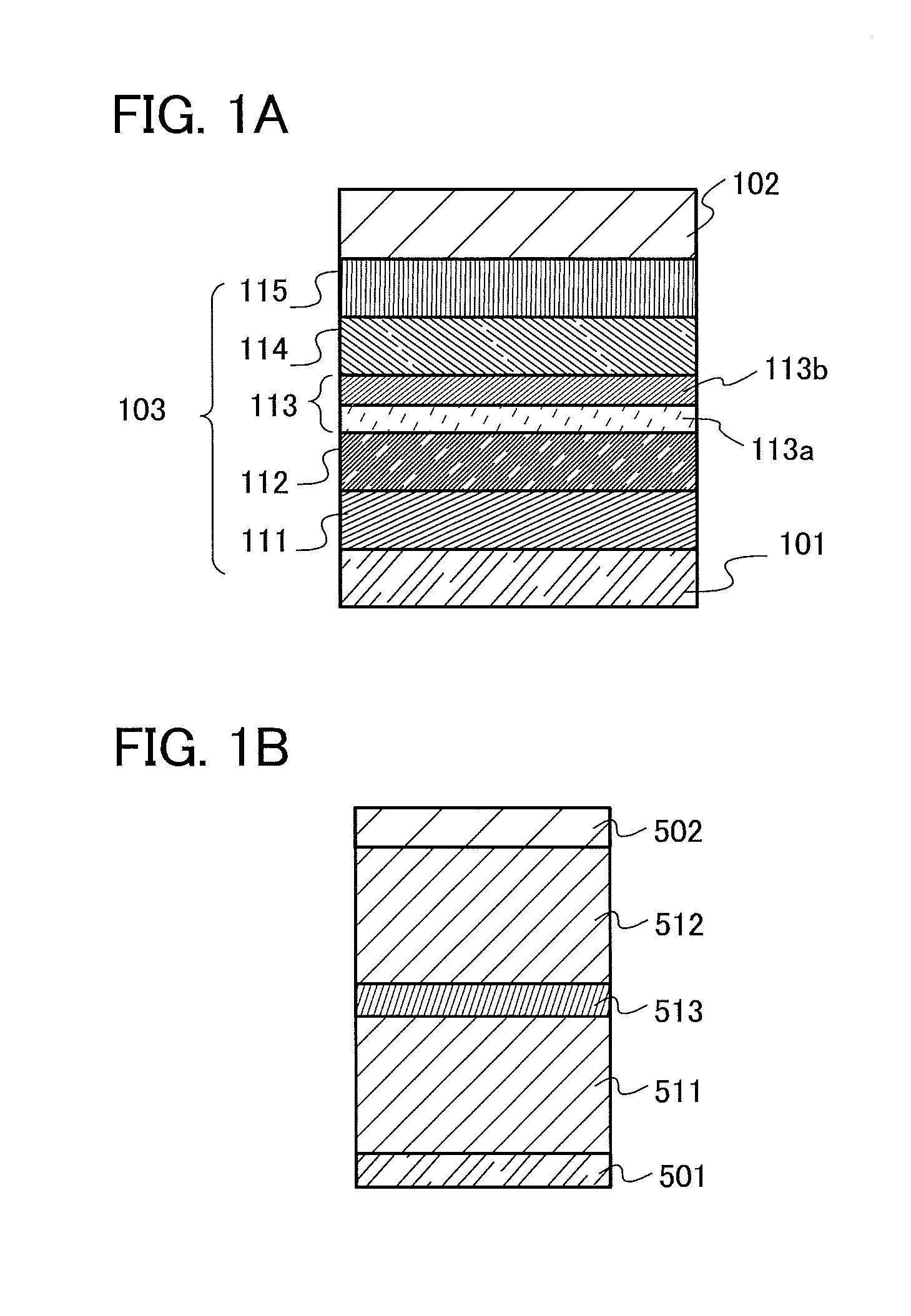
[0088]FIG. 1A is a diagram illustrating a light-emitting element of one embodiment of the present invention. The light-emitting element includes at least a pair of electrodes (a first electrode 101 and a second electrode 102) and an EL layer 103 including a light-emitting layer 113. In the light-emitting layer 113, a first light-emitting layer 113a and a second light-emitting layer 113b are stacked in contact with each other.

[0089]FIG. 1A also illustrates a hole-injection layer 111, a hole-transport layer 112, an electron-transport layer 114, and an electron-injection layer 115 in the EL layer 103. However, this stacked-layer structure is an example, and the structure of the EL layer 103 in the light-emitting element of one embodiment of the present invention is not limited thereto. Note that in FIG. 1A, the first electrode 101 functions as an anode, and the second electrode 102 functions as a cathode.

[0090]The first light-emitting layer 113a contains a first organic compound and a ...

embodiment 2

[0120]In this embodiment, a detailed example of the structure of the light-emitting element described in Embodiment 1 is described below with reference to FIG. 1A.

[0121]A light-emitting element in this embodiment includes, between a pair of electrodes, an EL layer including a plurality of layers. In this embodiment, the light-emitting element includes the first electrode 101, the second electrode 102, and the EL layer 103 provided between the first electrode 101 and the second electrode 102. Note that in this embodiment, the first electrode 101 functions as an anode and the second electrode 102 functions as a cathode. In other words, when voltage is applied between the first electrode 101 and the second electrode 102 so that the potential of the first electrode 101 is higher than that of the second electrode 102, light emission can be obtained.

[0122]Since the first electrode 101 functions as the anode, the first electrode 101 is preferably formed using any of metals, alloys, electri...

embodiment 3

[0177]In this embodiment, a light-emitting device including the light-emitting element described in Embodiment 1 or 2 is described.

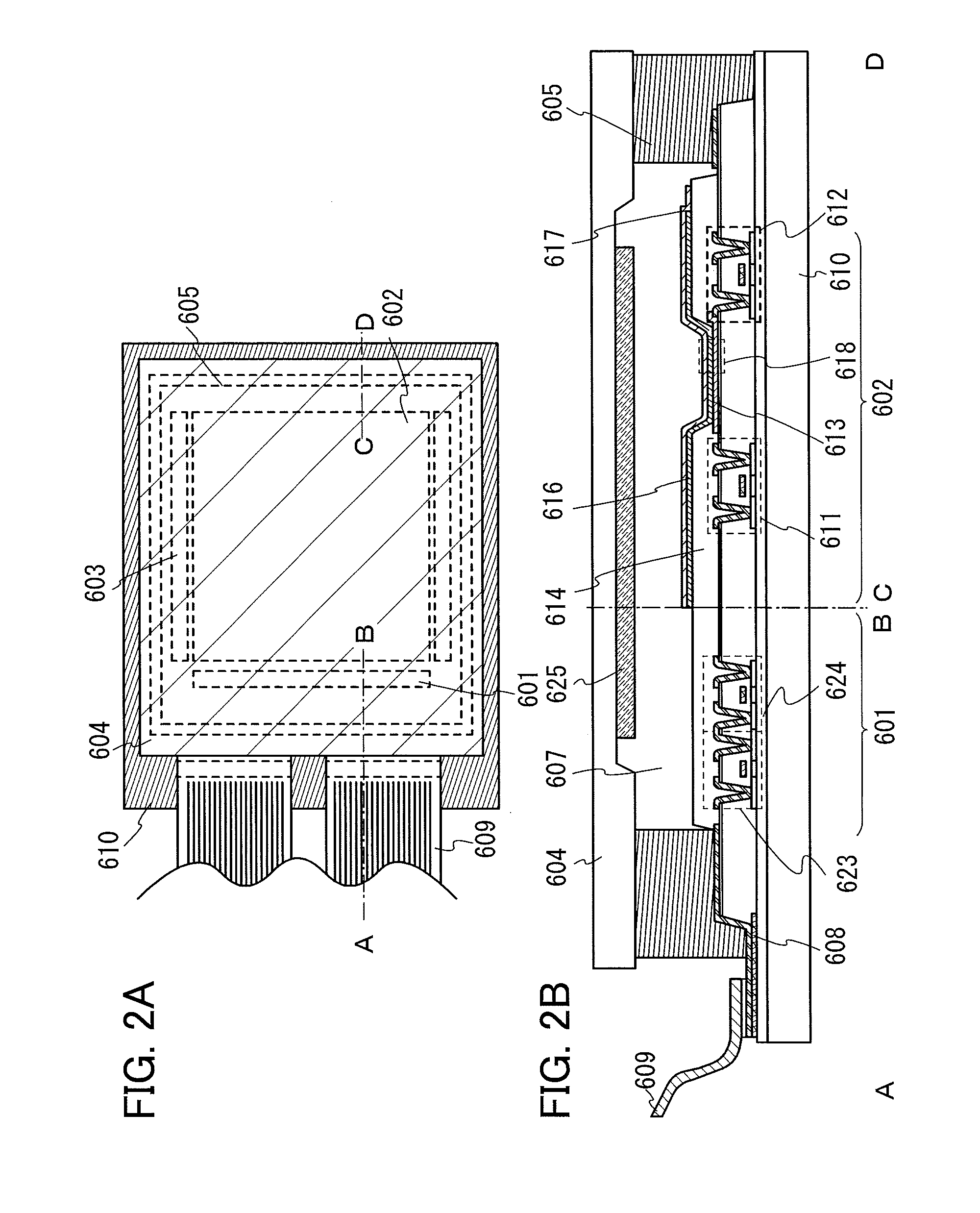
[0178]In this embodiment, the light-emitting device manufactured using the light-emitting element described in Embodiment 1 or 2 is described with reference to FIGS. 2A and 2B. Note that FIG. 2A is a top view illustrating the light-emitting device and FIG. 2B is a cross-sectional view of FIG. 2A taken along lines A-B and C-D. This light-emitting device includes a driver circuit portion (source line driver circuit) 601, a pixel portion 602, and a driver circuit portion (gate line driver circuit) 603, which are to control light emission of the light-emitting element and illustrated with dotted lines.

[0179]Moreover, a reference numeral 604 denotes a sealing substrate; 605, a sealing material; and 607, a space surrounded by the sealing material 605.

[0180]Note that a lead wiring 608 is a wiring for transmitting signals to be input to the source line driver ci...


PUM


Abstract

A multicolor light-emitting element using fluorescence and phosphorescence, which has a small number of manufacturing steps owing to a relatively small number of layers to be formed and is advantageous for practical application can be provided. In addition, a multicolor light-emitting element using fluorescence and phosphorescence, which has favorable emission efficiency is provided. A light-emitting element which includes a light-emitting layer having a stacked-layer structure of a first light-emitting layer exhibiting light emission from a first exciplex and a second light-emitting layer exhibiting phosphorescence is provided.

Description

TECHNICAL FIELD[0001]The present invention relates to a light-emitting element, a display device, a light-emitting device, an electronic appliance, and a lighting device each of which uses an organic compound as a light-emitting substance.BACKGROUND ART[0002]In recent years, research and development of a light-emitting element (organic EL element) which uses an organic compound and utilizes electroluminescence (EL) have been actively promoted. In the basic structure of such a light-emitting element, an organic compound layer containing a light-emitting substance (an EL layer) is interposed between a pair of electrodes. By voltage application to this element, light emission from the light-emitting substance can be obtained.[0003]Such a light-emitting element is a self-luminous element and has advantages over a liquid crystal display in having high pixel visibility and eliminating the need for backlights, for example; thus, such a light-emitting element is thought to be suitable for a...

Claims


Application Information

Patent Timeline
Patent Type & Authority Applications(United States)
IPC IPC(8): H01L51/50
CPCH01L51/504H10K85/341H10K85/346H10K85/342H10K50/13H10K50/11H10K2101/10H10K2101/20H01L2924/12044H10K50/81H10K50/82H10K85/633H10K85/636H10K85/6572H10K85/6576H10K85/615H10K85/624H10K85/626H10K2101/27H10K2101/90
Inventor SEO, SATOSHISEO, HIROMITAKAHASHI, TATSUYOSHIISHISONE, TAKAHIRO
Owner SEMICON ENERGY LAB CO LTD
Why Eureka
Try Eureka