Probe card, test apparatus having the probe card, and test method using the test apparatus

Active Publication Date: 2007-01-25
SAMSUNG ELECTRONICS CO LTD
View PDF4 Cites 15 Cited by
  • Summary
  • Abstract
  • Description
  • Claims
  • Application Information

AI Technical Summary

Benefits of technology

[0012] The present invention, therefore, provides a probe card capable of preventing deformation of

Problems solved by technology

However, since each chip formed on the wafer has a very small size, it is very difficult to directly connect a tester for applying a predetermined electrical signal to each chip.
However, in this case, the probe needles contacting the chip on the wafer are also heated to the high temperature, which to causes various problems.
First, the probe needles heated to the high temperature may be deformed, i.e., twisted, bent or the like.
Second, the probe needles heat

Method used


Image

  • Probe card, test apparatus having the probe card, and test method using the test apparatus
  • Probe card, test apparatus having the probe card, and test method using the test apparatus
  • Probe card, test apparatus having the probe card, and test method using the test apparatus

Examples


Example

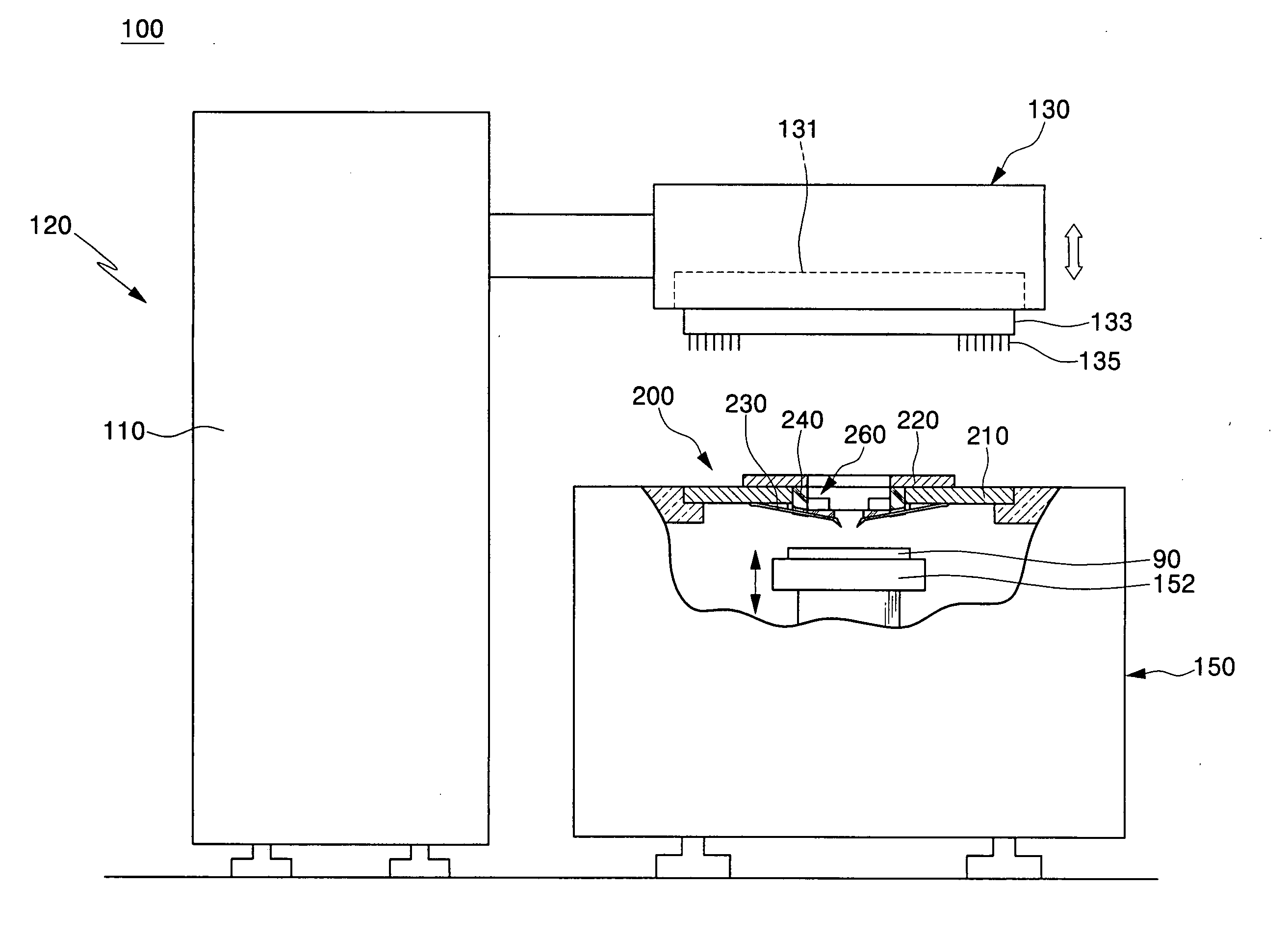
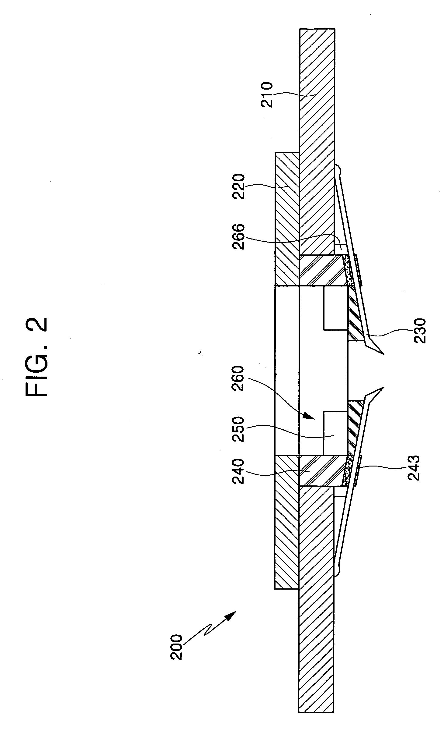
[0029]FIG. 1 is a side view of a test apparatus in accordance with an embodiment of the present invention, FIG. 2 is a cross-sectional view of a probe card of the test apparatus shown in FIG. 1, and FIG. 3 is a cross-sectional view of a cooling unit and a thermostat of a probe card in accordance with the present invention.

[0030] Referring to FIGS. 1 to 3, a test apparatus 100 in accordance with an embodiment of the present invention includes a tester 120 for generating a predetermined electrical signal, i.e., a test signal, to test a chip and transmitting the test signal to the chip, a prober 150 for moving a wafer 90 to allow the tester 120 to perform a test, and a probe card 200 functioning as an intermediate device for transmitting the signal generated from the tester 120 to the chip formed on the wafer 90.

[0031] Specifically, the tester 120 includes a test body 110, and a test head 130 raised and lowered from the test body 110 by a predetermined distance.

[0032] The test body ...


PUM


Abstract

Provided are a probe card, a test apparatus having the probe card, and a test method using the test apparatus. The probe card includes a probe substrate having a signal line, a probe needle connected to the signal line and fixed to the probe substrate, and a cooling unit for cooling the temperature of the probe needle. Therefore, the probe needles contacting each chip can be maintained at a certain low temperature without increasing the temperature. As a result, it is possible to pervent deformation of the probe needles and minimize an amount of impurities stuck to the probe needles.

Description

[0001] This application claims the benefit of Korean Patent Application No. 2005-0067376, filed Jul. 25, 2005, the contents of which are hereby incorporated herein by reference in their entirety. BACKGROUND OF THE INVENTION [0002] 1. Field of the Invention [0003] The present invention relates to an apparatus and method used in an electrical die sorting (EDS) process of a semiconductor test process, and more particularly, to a probe card that transmits an electrical signal for testing a chip to a chip pad on a wafer, a test apparatus having the probe card, and a test method using the test apparatus. [0004] 2. Description of Related Art [0005] Generally, a semiconductor manufacturing process includes a fabrication process for forming a plurality of chips on a wafer, an EDS process for testing electrical characteristics of each chip formed on the wafer, and an assembly process for individually separating good chips tested by the EDS process and packaging the chips to prevent the chips ...

Claims


Application Information

Patent Timeline
IPC IPC(8): G01R31/02
CPCG01R31/2891G01R1/067H01L22/00
Inventor BAE, YOUNG-GILPARK, SOON-JONGKIM, IN-SU
Owner SAMSUNG ELECTRONICS CO LTD
Why Eureka
Try Eureka