Liquid crystal display

a liquid crystal display and display technology, applied in non-linear optics, instruments, optics, etc., can solve the problem of difficult stabilization of bend configuration

Inactive Publication Date: 2007-01-25
TOSHIBA MOBILE DISPLAY CO LTD 50
View PDF4 Cites 8 Cited by
  • Summary
  • Abstract
  • Description
  • Claims
  • Application Information

AI Technical Summary

Benefits of technology

[0010] According to a first aspect of the present invention, there is provided a liquid crystal display comprising a back substrate which comprises a first substrate, a first electrode disposed on a main surface of the first substrate, and a first alignment layer covering the first electrode and including a first corrugated surface at a position of the first electrode, wherein the first corrugated surface includes first upslopes and first downslopes steeper than the first upslopes or first vertical surfaces which are alternately joined in an in-plane direction parallel to the main surface of the first substrate, and wherein a period of the first upslope in the in-plane direction is 1 μm or less, a front substrate which comprises a second substrate facing the first alignment layer, a second electrode disposed on a main surface of the second substrate facing the first alignment layer, and a second alignment layer covering the second electrode and including a second corrugated surface at a position of the second electrode, wherein the second corrugated surface includes second upslopes and second downslopes steeper than the second upslopes or second vertical surfaces which are alternately joined in the in-plane direction, and wherein a period of the second upslope in the in-plane direction is 1 μm or less, and an optical filter layer interposed between the back and front substrates and containing a liquid crystal material which forms a bend configuration when a voltage is applied between the first and second electrodes.

Problems solved by technology

However, bend configuration is difficult to stabilize as will be explained below.

Method used


Image

  • Liquid crystal display
  • Liquid crystal display
  • Liquid crystal display

Examples


example 1

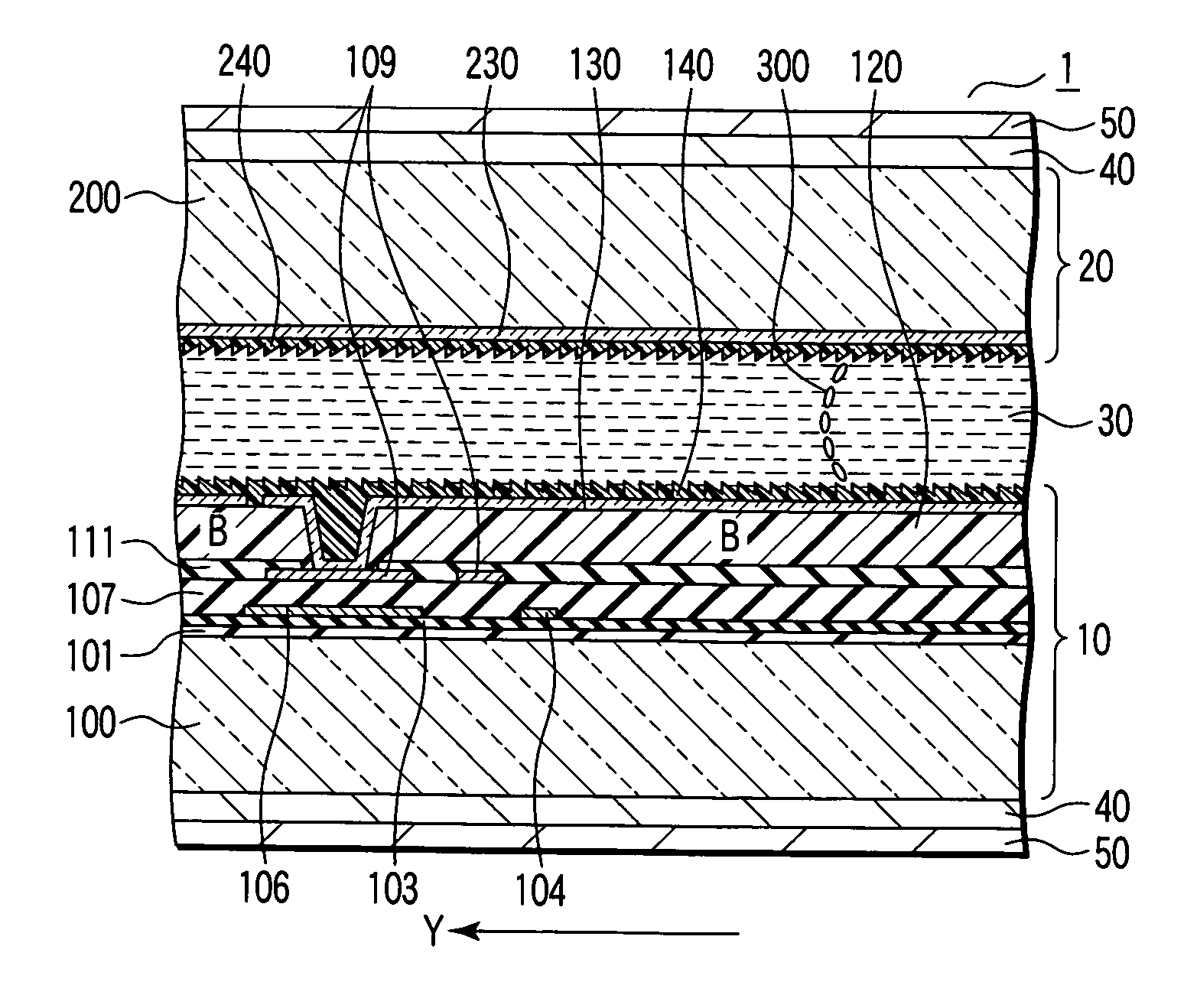
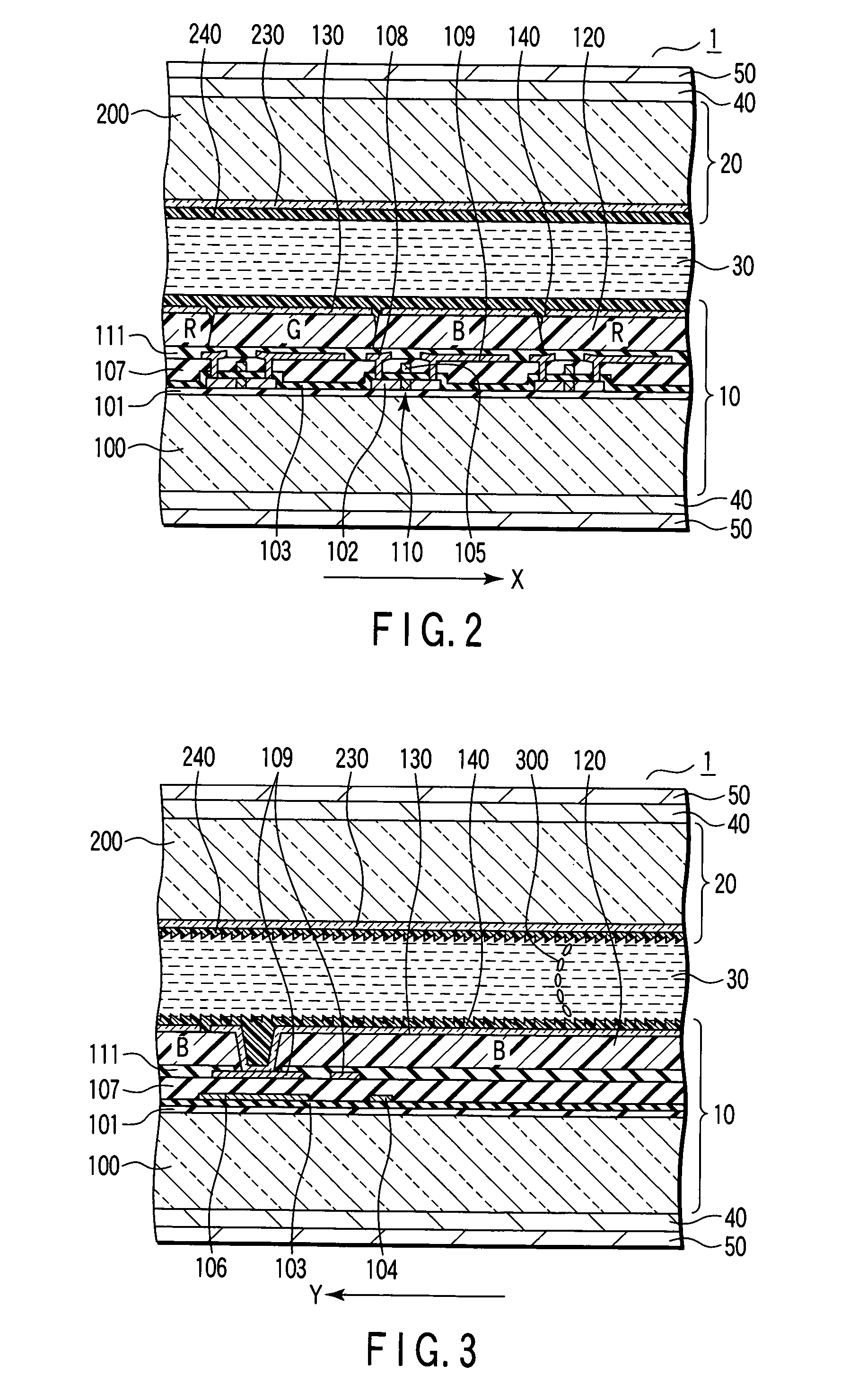
[0166] In this example, the OCB-mode liquid crystal display shown in FIGS. 1 to 3 was manufactured by the following method. Note that the structure shown in FIG. 13 was used in this liquid crystal display, and the period P and inclination angle α of the alignment layers 140 and 240 were set at about 0.15 μm and 45°, respectively. In this example, the optical compensation film 40 was formed not on the outer surface of the back substrate 10, but only on the outer surface of the front substrate 20.

[0167] First, a structure from an undercoat layer 101 to pixel electrodes 130 was formed on a 0.5-mm-thick glass substrate 100. On this structure, an SiO2 layer and acrylic resin layer were sequentially formed as a planarizing layer 150. Also, a common electrode 230 was formed on a 0.5-mm-thick glass substrate 200.

[0168] Then, each of the planarizing layer 150 and common electrode 230 was spin-coated with Optomer-AL3456 manufactured by JSR, thereby forming a 0.8-μm-thick polyimide resin lay...

example 2

[0181] The liquid crystal display shown in FIGS. 1 to 3 was manufactured following the same procedures as explained in Example 1 except that the period P of each of the alignment layers 140 and 240 was set to about 0.25 μm.

[0182] In this example, the maximum value Dmax and minimum value Dmin Of the cell gap were about 8.0 μm and about 7.5 μm, respectively. Also, the maximum value RON−max of the optical retardation of the optical filter layer 30 in the on state was checked by using an ellipsometer, and found to be about 26 nm. That is, the maximum value Dmax, minimum value Dmin, and maximum value RON−max satisfy the relationship indicated by inequality (1). In addition, the maximum value εmjr of the relative dielectric constant of the liquid crystal material was about 19, and the relative dielectric constant εAL of the alignment layers 140 and 240 was about 4.0. Accordingly, the maximum value Dmax, minimum value Dmin, maximum value RON−max, maximum value εmjr, and relative dielectri...

example 3

[0185] In this example, the OCB-mode liquid crystal display shown in FIGS. 15 to 17 was manufactured by the following method. Note that in this liquid crystal display, the period P and inclination angle α of the alignment layers 140 and 240 were set to about 0.90 μm and 30°, respectively.

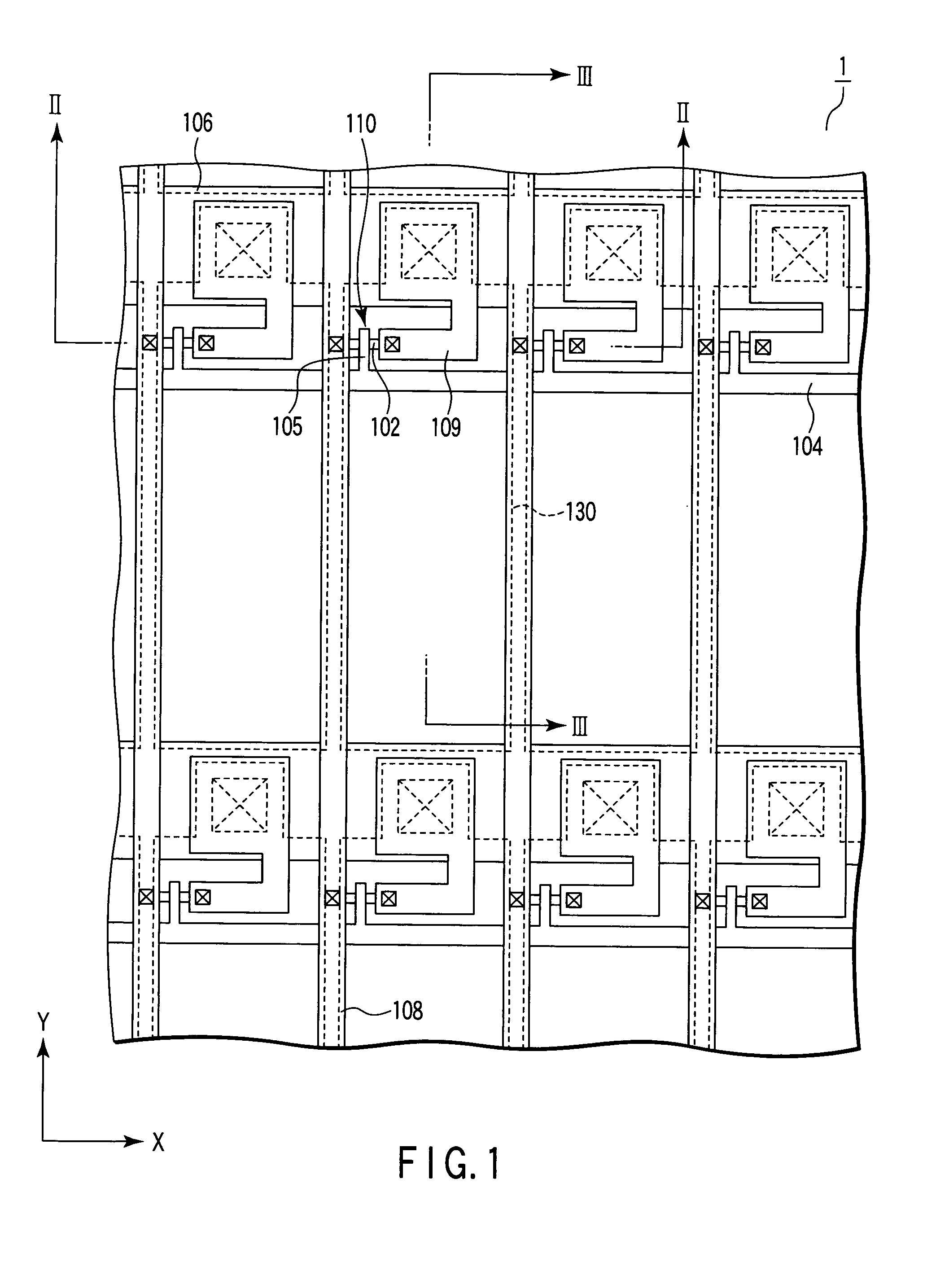
[0186] First, X electrodes 130 made of ITO were formed on a 0.5-mm-thick glass substrate 100. A planarizing layer 150 made of SiO2 was formed on this structure.

[0187] Also, a color filter 220 and Y electrodes 230 made of ITO were formed on a 0.5-mm-thick glass substrate 200. A planarizing layer 250 made of SiO2 was formed on this structure.

[0188] Then, 0.6-μm-thick inorganic insulating layers made of TaOx were formed on the planarizing layers 150 and 250. These inorganic insulating layers were obtained by forming films by RF sputtering using Ta2O5 as a sputter target, and annealing the films at 200° C. for 1 hour. At the same time these inorganic insulating layers were formed, another inorganic i...


PUM

PropertyMeasurementUnit
inclination angleaaaaaaaaaa
pretilt angleaaaaaaaaaa

Abstract

A liquid crystal display includes a back substrate, a front substrate, and an optical filter layer interposed therebetween. The optical filter layer contains a liquid crystal material which forms a bend configuration when a voltage is applied between electrodes of the back and front substrates. The electrodes of the back and front substrates are covered with alignment layers which include corrugated surfaces at positions of the electrodes. Each corrugated surface includes upslopes and downslopes steeper than the upslopes or vertical surfaces which are alternately joined.

Description

CROSS-REFERENCE TO RELATED APPLICATIONS [0001] This application is based upon and claims the benefit of priority from prior Japanese Patent Application No. 2004-380590, filed Dec. 28, 2004, the entire contents of which are incorporated herein by reference. BACKGROUND OF THE INVENTION [0002] 1. Field of the Invention [0003] The present invention relates to a liquid crystal display which employs a display mode utilizing birefringence and, more particularly, to a liquid crystal display employing a display mode in which a liquid crystal material forms bend configuration. [0004] 2. Description of the Related Art [0005] In a liquid crystal display using an optically compensated birefringence (OCB) mode, a liquid crystal material is caused to form bend configuration, and the tilt angles of liquid crystal molecules are changed near each alignment layer, thereby changing the optical retardation of an optical filter layer. Because of utilizing bend configuration, the OCB-mode is one of the di...

Claims


Application Information

Patent Timeline
Patent Type & Authority Applications(United States)
IPC IPC(8): G02F1/1337
CPCG02F1/13378G02F2001/133776G02F2001/133773G02F1/1393G02F1/133773G02F1/133776G02F1/1337
Inventor KIZU, YUKOHASEGAWA, REIHIOKI, TSUYOSHI
Owner TOSHIBA MOBILE DISPLAY CO LTD 50
Why Eureka
Try Eureka