Organic light emitting display with circuit measuring pad and method of fabricating the same

a technology of organic light and circuit, which is applied in the manufacture of electrode systems, electric discharge tubes/lamps, and testing/measurement of semiconductor/solid-state devices, etc., can solve the problems of low reliability of oled and failure of oled, and achieve the effect of improving the reliability of a display

Active Publication Date: 2007-01-25
SAMSUNG DISPLAY CO LTD
View PDF3 Cites 19 Cited by
  • Summary
  • Abstract
  • Description
  • Claims
  • Application Information

AI Technical Summary

Benefits of technology

[0010] The present invention, therefore, solves aforementioned problems associated with conventional devices by providing a circuit measuring pad which may prevent a short circuit between the circuit measuring pad and an opposite electrode to thereby improve reliability of a display, an OLED with the circuit measuring pad, and method of fabricating the same.

Problems solved by technology

However, the driving circuit measuring pad may cause a short circuit with an opposite electrode formed on the display region of the OLED, leading to failure of the OLED and low reliability of the OLED.

Method used


Image

  • Organic light emitting display with circuit measuring pad and method of fabricating the same
  • Organic light emitting display with circuit measuring pad and method of fabricating the same
  • Organic light emitting display with circuit measuring pad and method of fabricating the same

Examples


first embodiment

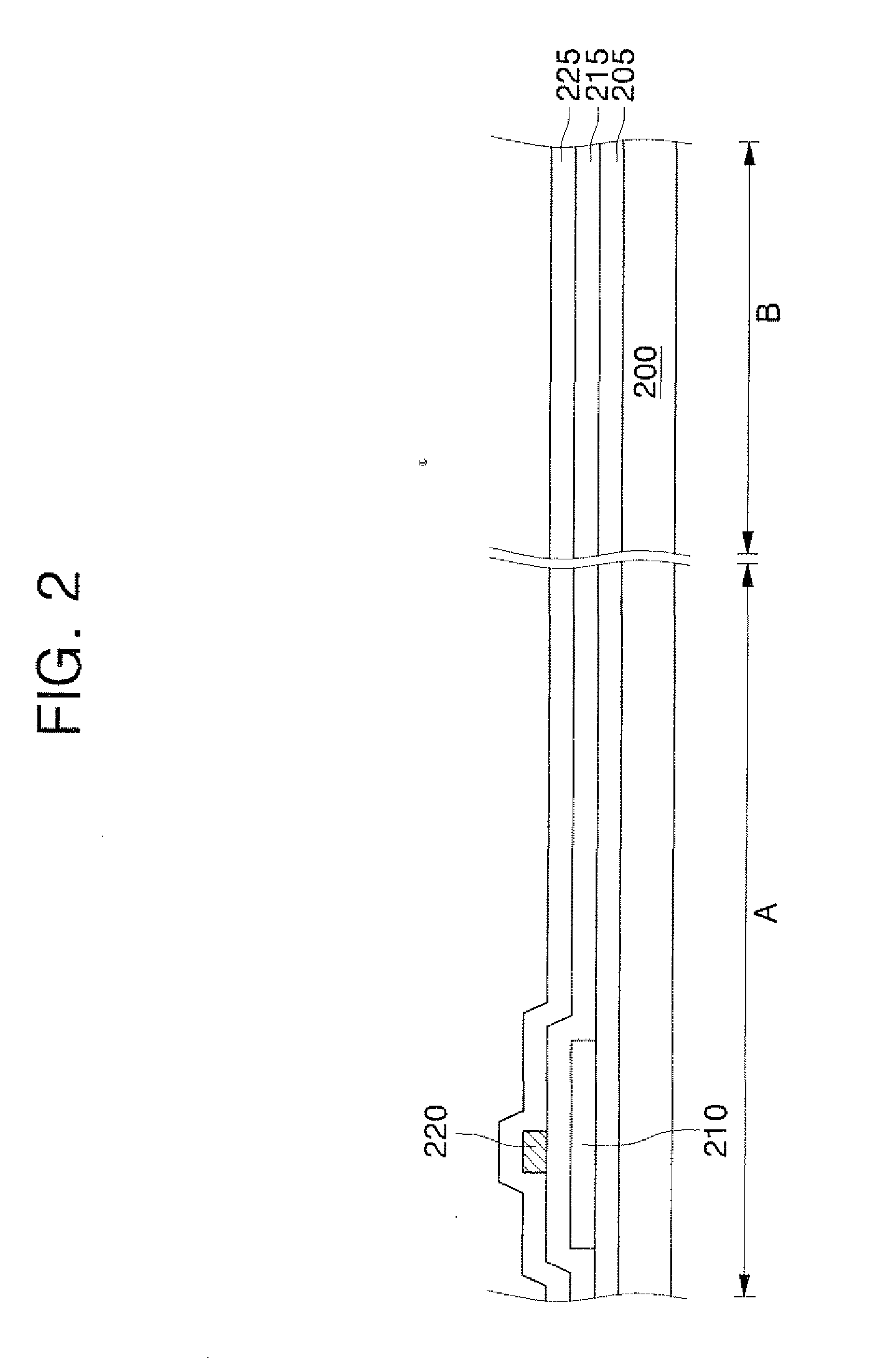
[0022]FIG. 5 is a cross-sectional view of an OLED according to the present invention, taken along the line I-I′ in FIG. 1.

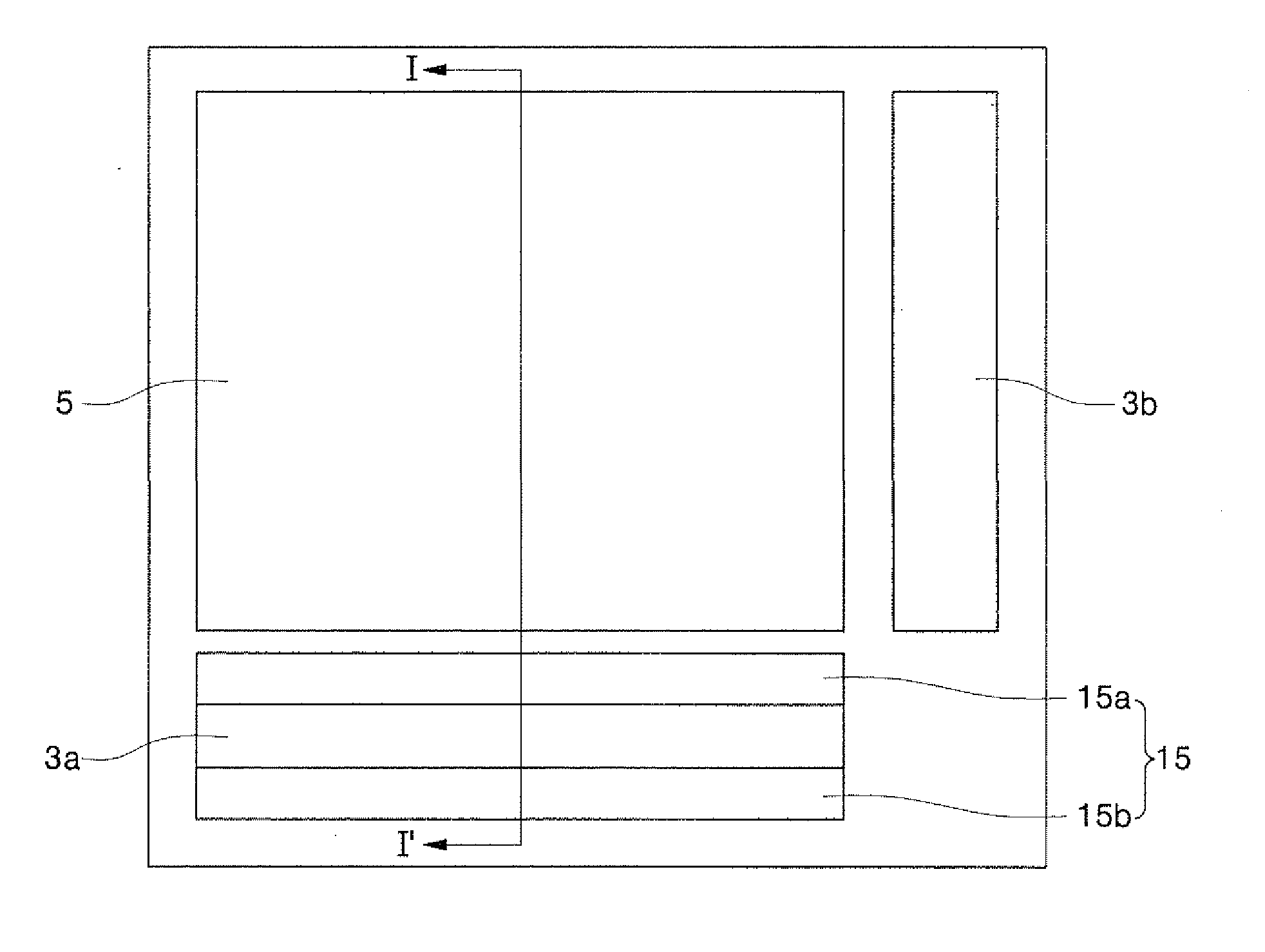
[0023] Referring to FIG. 5, a substrate 200 includes a display region A and a circuit measuring pad region B.

[0024] A buffer layer 205 is arranged on the display region A and the circuit measuring pad region B, and a TFT is arranged on the buffer layer 205 of the display region A. The TFT includes a semiconductor layer 210, a gate insulating layer 215, a gate electrode 220, an inter insulating layer 220, and source and drain electrodes 230a and 230b.

[0025] Insulating layers which are deposited at the same time as the gate insulating layer 215 and the interlayer insulating layer 225 are arranged on the buffer layer 205 of the circuit measuring pad region B.

[0026] A first conductive layer 230c is arranged on the interlayer insulating layer 225 of the circuit measuring pad region B.

[0027] A first insulating layer is arranged on the source and drain electrodes 23...

second embodiment

[0058]FIG. 6 is a cross-sectional view of an OLED according to the present invention.

[0059] Referring to FIG. 6, like the first embodiment of the present invention, a substrate 300 includes a display region A on which source and drain electrodes 330a and 330b are arranged and a circuit measuring pad region B on which a first conductive layer 330c is arranged.

[0060] A first insulating layer is arranged on the source and drain electrodes 330a and 330b and the first conductive layer 330c. The first insulating layer may be a passivation layer 335. In the second embodiment of the present invention, a planarization layer 340 is formed above only the display region A except the circuit measuring pad region B.

[0061] A taper angle θ1 of a second via hole may be 50° or less.

[0062] Thickness of a second conductive layer 350b may be in a range of 100 to 1,000 Å.

[0063] A taper angle θ2 of an edge of the second conductive layer 350b may be 50° or less.

[0064] A second insulating layer 360b ar...


PUM


Abstract

An organic light emitting display and method of fabricating the same are disclosed. The light emitting display includes: a substrate having a display region and a circuit measuring pad region; source and drain electrodes arranged above the display region and a first conductive layer arranged above the circuit measuring pad region on the same layer as the source and drain electrodes; a first insulating layer on the source and drain electrodes and the first conductive layer; first and second via holes formed in the first insulating layer, the first via hole exposing the source or drain electrode, the second via hole exposing the first conductive layer; a pixel electrode contacting the source or drain electrode through the first via hole, and a second conductive layer contacting the first conductive layer through the second via hole; and a pixel defining layer which exposes the pixel electrode and formed on the second conductive layer.

Description

CROSS-REFERENCE TO RELATED APPLICATIONS [0001] This application is a divisional of prior application Ser. No. 11 / 019,457, filed Dec. 23, 2004, which claims priority to and the benefit of Korean Patent Application No. 10-2004-0070087, filed Sep. 2, 2004, which are all hereby incorporated by reference for all purposes as if fully set forth herein. BACKGROUND OF THE INVENTION [0002] 1. Field of the Invention [0003] The present invention relates to an organic light emitting display with a circuit measuring pad and method of fabricating the same and, more particularly, to an organic light emitting display with a circuit measuring pad which may prevent a short circuit between the circuit measuring pad and an opposite electrode and method of fabricating the same. [0004] 2. Description of the Related Art [0005] Among flat panel displays, an organic light emitting display (OLED) has a fast response speed of 1 ms or less, low power consumption, and a wide viewing angle due to an emissive disp...

Claims


Application Information

Patent Timeline
Patent Type & Authority Applications(United States)
IPC IPC(8): H01J9/24H01J9/00H01L21/66H05B44/00H01L27/32H01L51/56
CPCH01L27/3246H01L51/56H01L27/3276H01L27/3258H10K59/122H10K59/124H10K59/131H10K71/00H10K71/70H05B33/00H05B33/10
Inventor KIM, MU-HYUNKIM, KEUM-NAM
Owner SAMSUNG DISPLAY CO LTD
Why Eureka
Try Eureka