

Mesoscale and microscale device fabrication methods using split structures and alignment elements
a technology of split structure and alignment elements, applied in waveguides, waveguide types, instruments, etc., can solve the problems of affecting affecting the separation of masking materials from substrates, and affecting the separation of masking materials. , to achieve the effect of reducing the separation time between structural and sacrificial materials
- Summary
- Abstract
- Description
- Claims
- Application Information
AI Technical Summary
Benefits of technology
Problems solved by technology
Method used
Image

Examples
Embodiment Construction
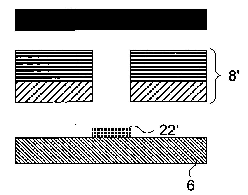
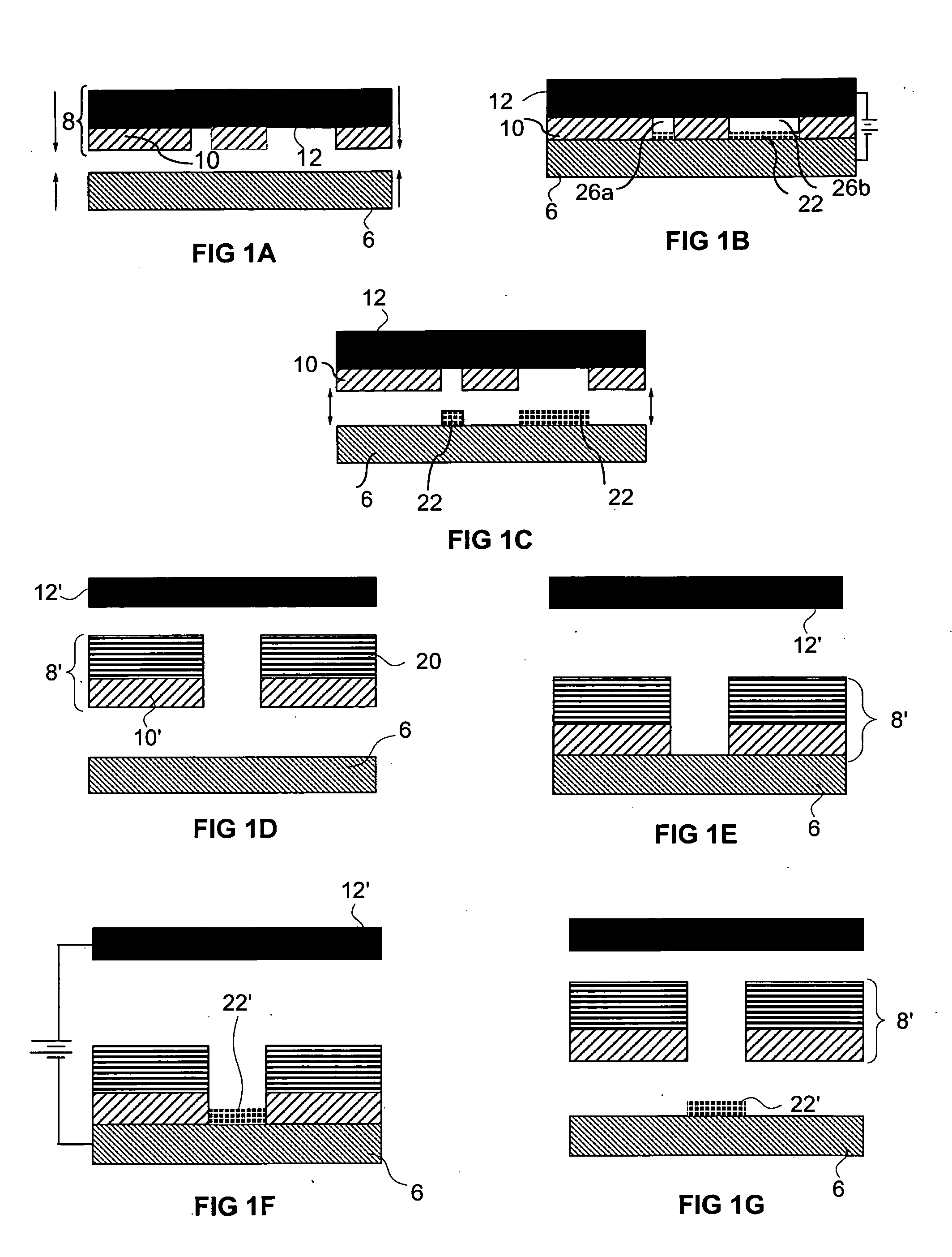
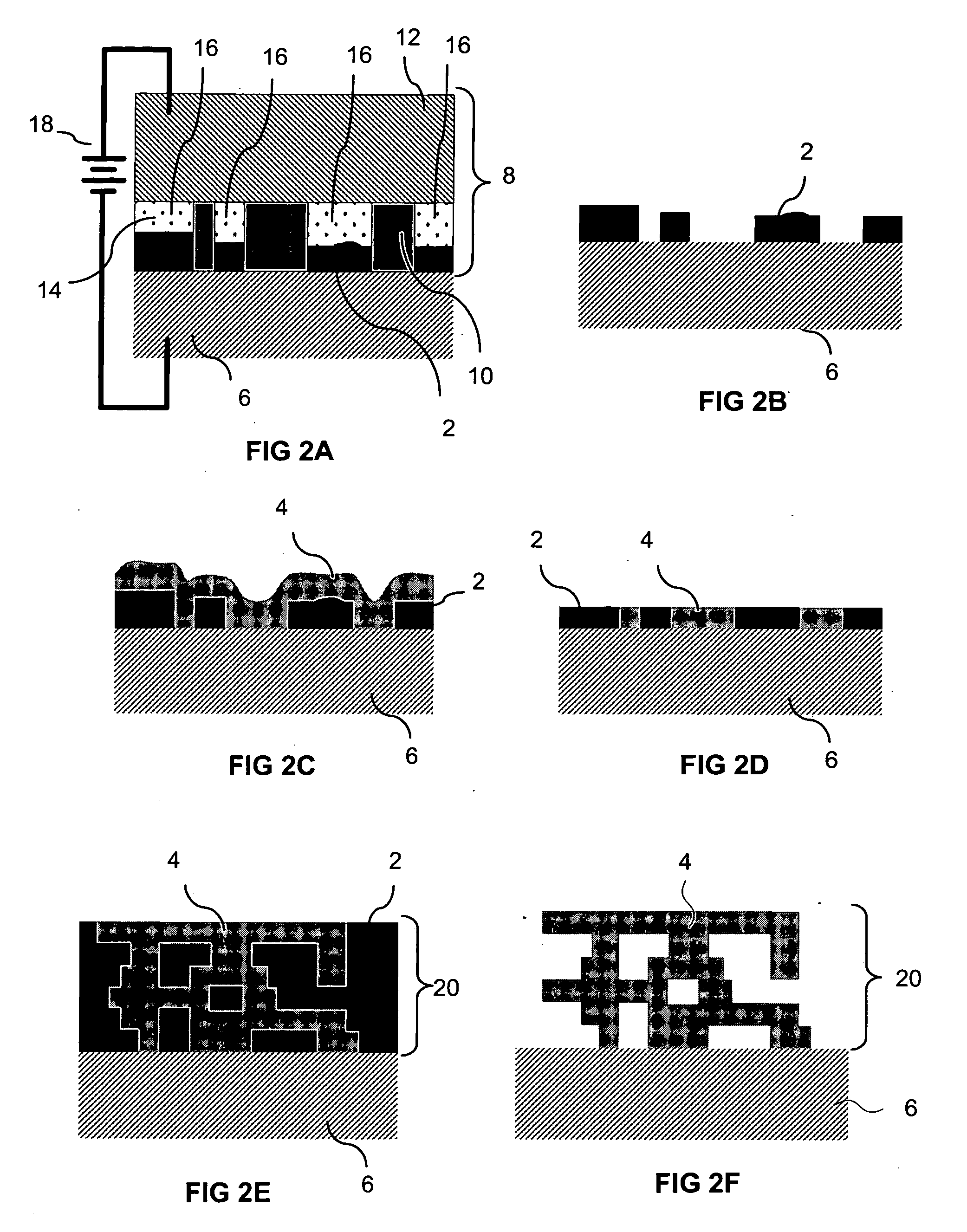
[0064]FIGS. 1A-1G, 2A-2F, and 3A-3C illustrate various features of one form of electrochemical fabrication. Other electrochemical fabrication techniques are set forth in the '630 patent referenced above, in the various previously incorporated publications, in various other patents and patent applications incorporated herein by reference. Still others may be derived from combinations of various approaches described in these publications, patents, and applications, or are otherwise known or ascertainable by those of skill in the art from the teachings set forth herein. All of these techniques may be combined with those of the various embodiments of various aspects of the invention to yield enhanced embodiments. Still other embodiments may be derived from combinations of the various embodiments explicitly set forth herein.
[0065]FIGS. 4A-4G illustrate various stages in the formation of a single layer of a multi-layer fabrication process where a second metal is deposited on a first meta...
PUM
| Property | Measurement | Unit |
|---|---|---|
| Aspect Ratio | aaaaa | aaaaa |
| thicknesses | aaaaa | aaaaa |
| thicknesses | aaaaa | aaaaa |
Abstract
Description
Claims
Application Information