Adopting feature of buried electrically conductive layer in dielectrics for electrical anti-fuse application

Inactive Publication Date: 2007-02-22
GLOBALFOUNDRIES INC
View PDF10 Cites 24 Cited by
  • Summary
  • Abstract
  • Description
  • Claims
  • Application Information

AI Technical Summary

Benefits of technology

[0011] One advantage of the present invention over the prior art is that no extra layer of anti-fuse material is required and the inventive method is compatible with current processing without requiring extra critical masking. The fabrication costs of the inventive method are therefore lower. In addition, and unlike prior art structures, the inventive structure does not require a sandwiched anti-fuse material layer between two ‘disconnected’ conductive materials. Thus, the inventive structure and method offer more flexibility for circuit design than the prior art anti-fuse structures described herein.
[0012] In general terms, the present invention provides a semiconductor structure comprising:
[0013] an insulator including at least a pair of adjacent interconnects, each interconnect of said pair includes a buried electrically conductive, e.g., metallic, layer embedded in a surface of said insulator and surrounding a portion of each respective interconnect, sa

Problems solved by technology

That is, the electrical resistance between these original interconnects starts decreasing when two adjac

Method used


Image

  • Adopting feature of buried electrically conductive layer in dielectrics for electrical anti-fuse application
  • Adopting feature of buried electrically conductive layer in dielectrics for electrical anti-fuse application
  • Adopting feature of buried electrically conductive layer in dielectrics for electrical anti-fuse application

Examples


Example

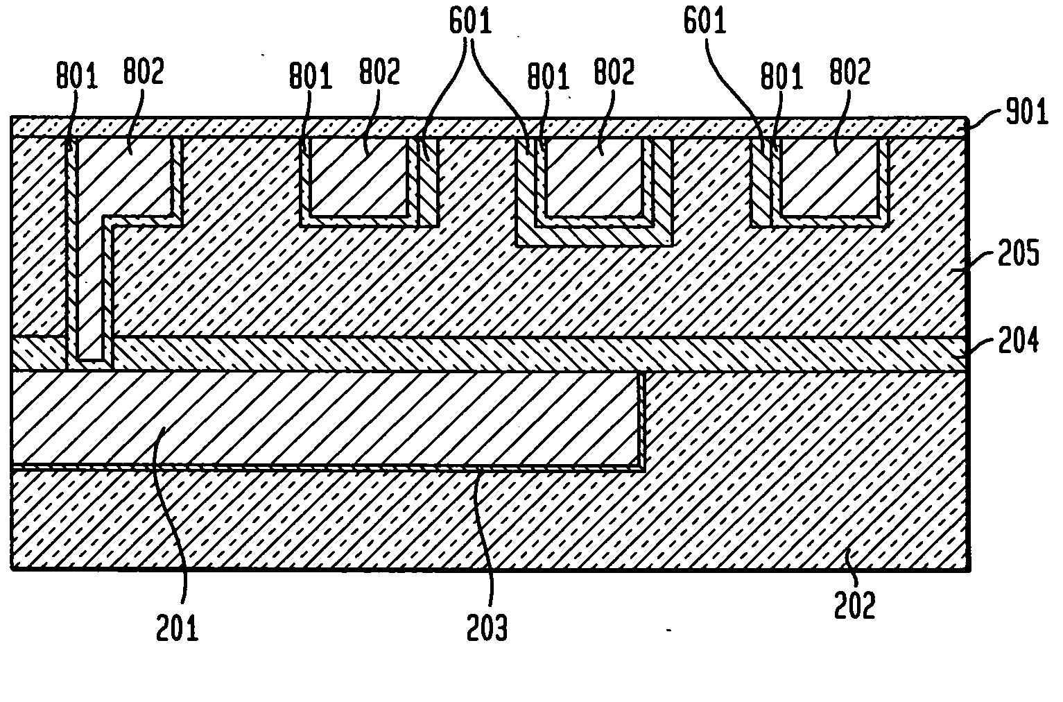
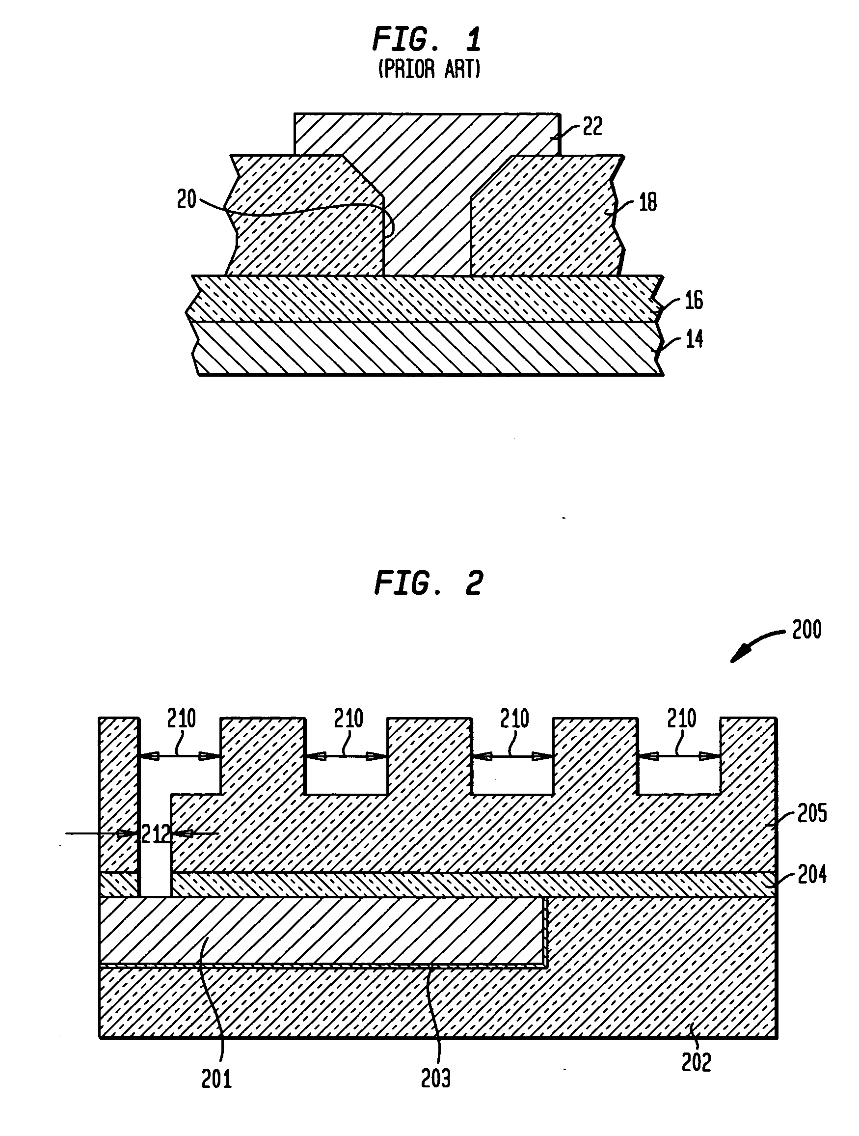
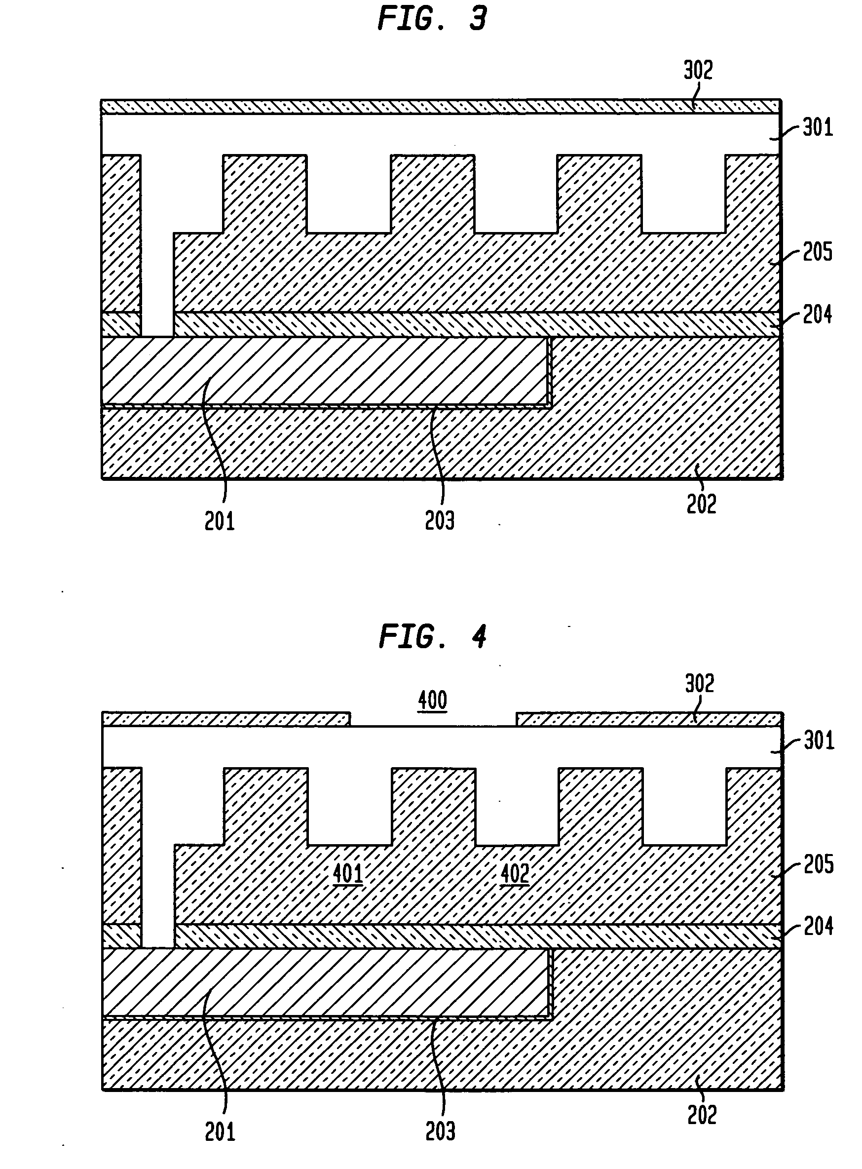
[0019] The present invention, which provides an anti-fuse structure including a specially modified anti-fuse material (or the buried electrically conductive) layer and a method of fabricating the same, will now be described in greater detail by referring to the following discussion and drawings that accompany the present application. It is noted that the drawings are provided for illustrative purposes and, as such, the drawings are not drawn to scale.

[0020] As stated above, the present invention provides an anti-fuse structure that includes a buried electrically conductive layer as an anti-fuse as well as a method of forming such an anti-fuse structure. According to the present invention, the inventive anti-fuse structure comprises regions of leaky dielectric between interconnects. The term “leaky dielectric” is used in the present application to describe a region of dielectric material between adjacent interconnects, and the region of dielectric is embedded with an electrically co...


PUM


Abstract

An anti-fuse structure that included a buried electrically conductive, e.g., metallic layer as an anti-fuse material as well as a method of forming such an anti-fuse structure are provided. According to the present invention, the inventive anti-fuse structure comprises regions of leaky dielectric between interconnects. The resistance between these original interconnects starts decreasing when two adjacent interconnects are biased and causes a time-dependent dielectric breakdown, TDDB, phenomenon to occur. Decreasing of the resistance between adjacent interconnects can also be expedited via increasing the local temperature.

Description

FIELD OF THE INVENTION [0001] The present invention relates to a semiconductor structure, and more particularly to an anti-fuse structure. Specifically, the present invention provides an anti-fuse structure including a buried electrically conductive layer, e.g., a buried metal layer, in a dielectric for electrical anti-fuse application. The present invention also provides a method of fabricating such an anti-fuse structure. BACKGROUND OF THE INVENTION [0002] Anti-fuse structures have been used in the semiconductor industry for memory related applications, such as, for example, field programmable gate arrays and programmable read-only memories. Prior art anti-fuse structures typically include a material which initially has a high resistance, but can be converted into a lower resistance material upon application of certain processes. For example, an unprogrammable anti-fuse type gate array can be programmed by causing selective anti-fuses to become conductive. [0003]FIG. 1 is a cross-...

Claims


Application Information

Patent Timeline
IPC IPC(8): H01L23/52H01L23/48H01L29/40
CPCH01L21/76843H01L21/76844H01L23/5252H01L2924/0002H01L2924/00
Inventor YANG, CHIH-CHAOCLEVENGER, LAWRENCE A.DALTON, TIMOTHY J.FULLER, NICHOLAS C.HSU, LOUIS C.
Owner GLOBALFOUNDRIES INC
Why Eureka
Try Eureka