Electro-optical device, method of testing the same, and electronic apparatus

Active Publication Date: 2007-02-22
SEIKO EPSON CORP
View PDF3 Cites 15 Cited by
  • Summary
  • Abstract
  • Description
  • Claims
  • Application Information

AI Technical Summary

Benefits of technology

[0010] An advantage of some aspects of the invention is that it provides an electro-optical device capable of easily performing a test after an element substrate and a counter substrate are bonded to each other and having a small size, a method of testing the electro-optical device, and an electronic apparatus including the electro-optical device.

Problems solved by technology

That is, when the size of the element substrate is reduced, it is practically difficult to bring the probe into contact with the test terminals to perform their test.
More specifically, in the portion of the peripheral region of the element substrate, the second test terminals are completely covered with the counter substrate, or they are covered with the counter substrate so that probing is difficult in plan view.

Method used


Image

  • Electro-optical device, method of testing the same, and electronic apparatus
  • Electro-optical device, method of testing the same, and electronic apparatus
  • Electro-optical device, method of testing the same, and electronic apparatus

Examples


Embodiment Construction

[0072] Preferred embodiments of the invention will be described with reference to the accompanying drawings. In the following embodiment, an electro-optical device of the invention is applied to a liquid crystal display device.

Overall Structure of Liquid Crystal Display Device

[0073] First, the overall structure of a liquid crystal display device according to an embodiment of the invention will be described with reference to FIGS. 1 to 3.

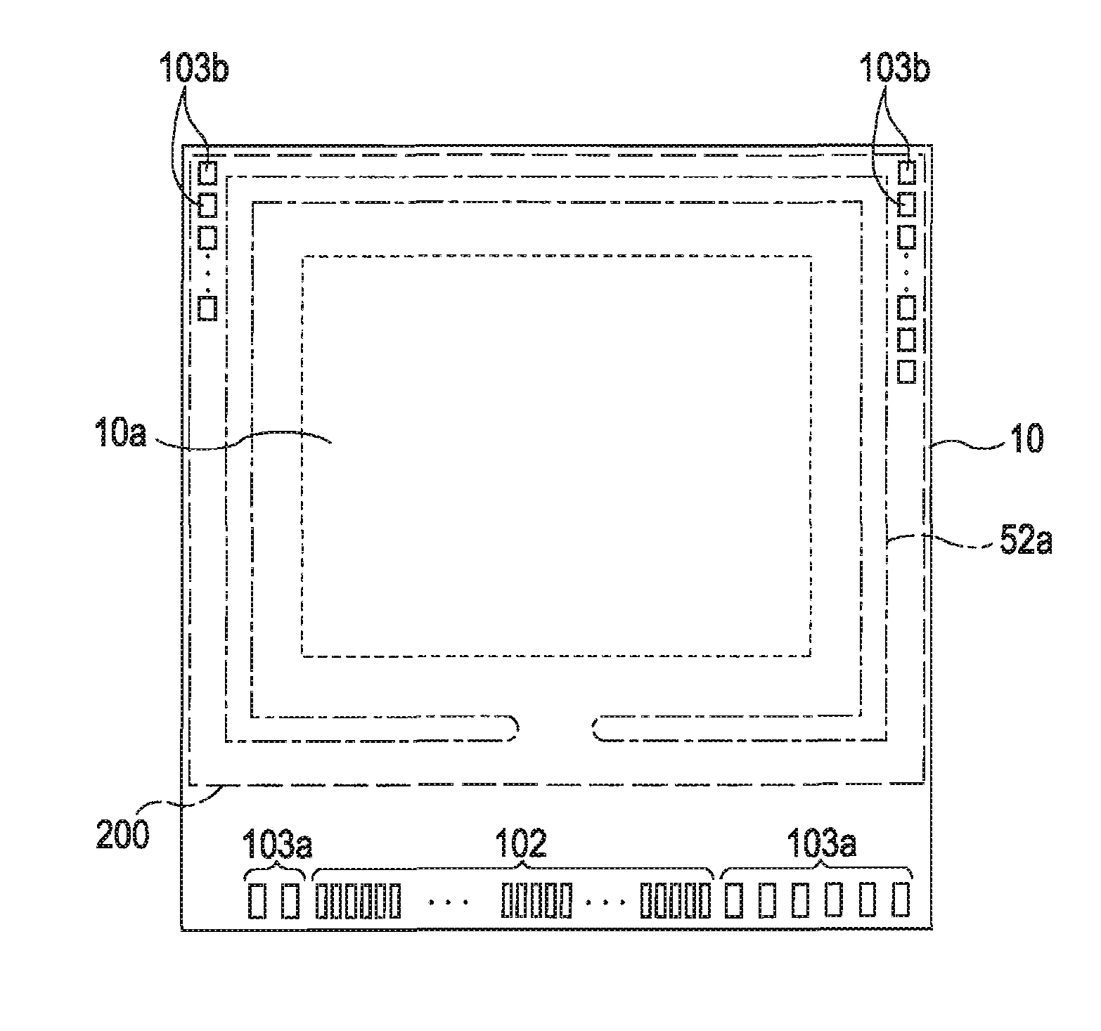
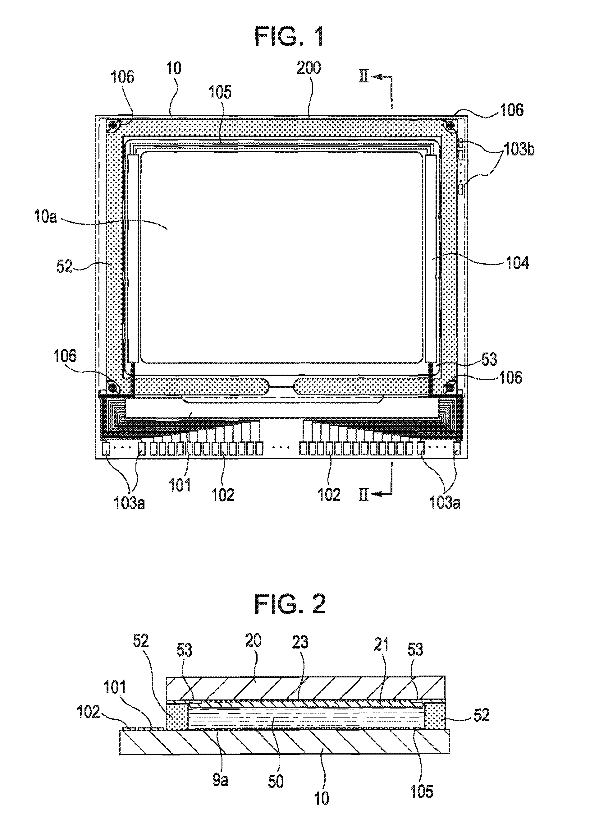
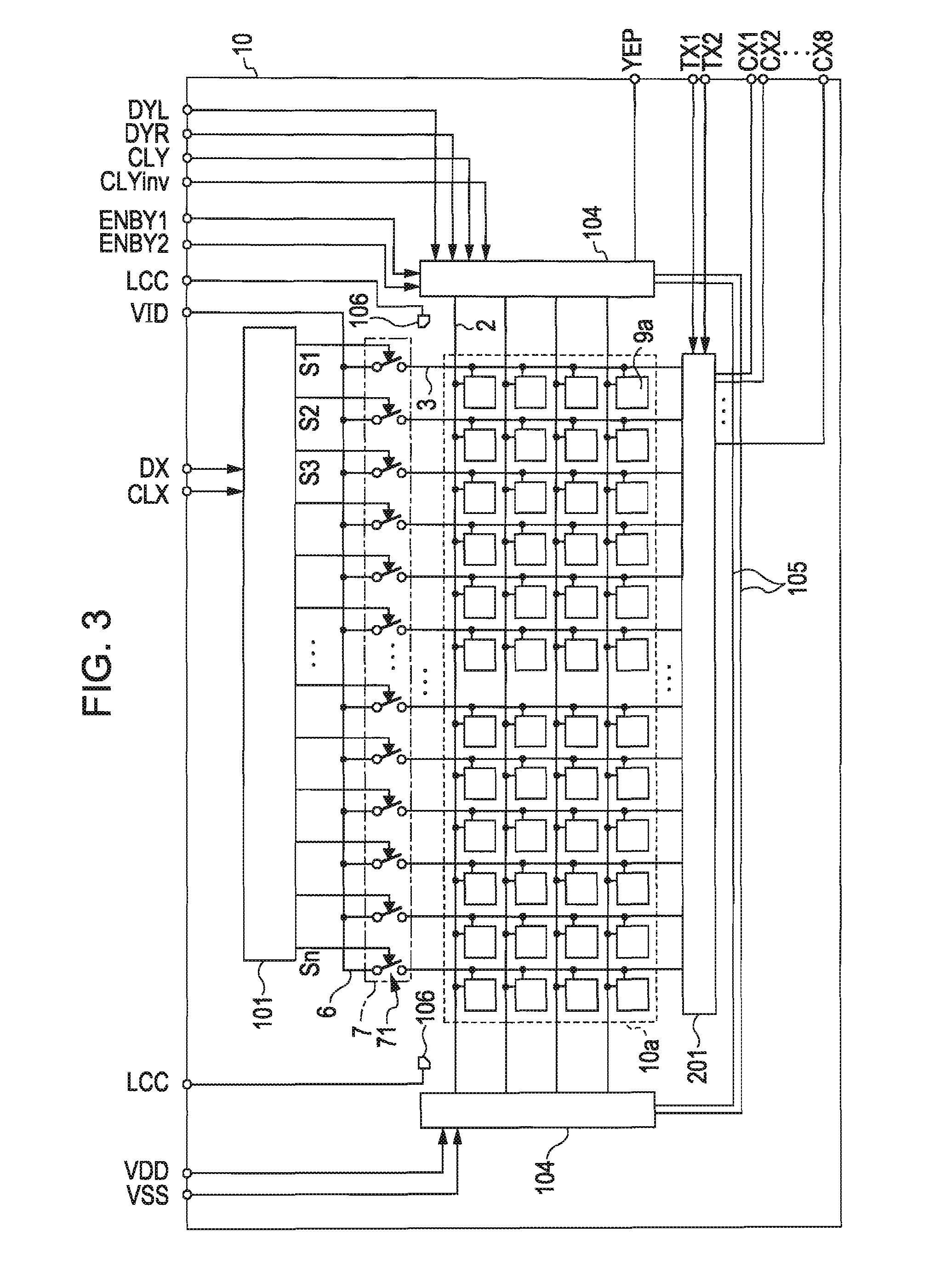
[0074]FIG. 1 is a plan view of the liquid crystal display device, as viewed from a counter substrate, and FIG. 2 is a cross-sectional view taken along the line II-II of FIG. 1. In FIGS. 1 and 2, the liquid crystal display device includes a TFT array substrate 10, which is an example of an ‘element substrate’ according to the invention, and a counter substrate 20 opposite to the TFT array substrate 10. In FIG. 1, the arrangement of the counter substrate 20 with respect to the TFT array substrate 10 is represented by a region that is surrounded by ...


PUM

PropertyMeasurementUnit
resistanceaaaaaaaaaa
distance d1aaaaaaaaaaa
distance d1baaaaaaaaaa

Abstract

An electro-optical device includes: a counter substrate; an element substrate comprising a protruding region protruding from one side of the counter substrate and being bonded to the counter substrate; a plurality of pixel units that are arranged in a pixel region on the element substrate; a plurality of external circuit connecting terminals which are arranged in the protruding region on the element substrate and to which various signals including image signals and control signals for allowing the plurality of pixel units to display an image are supplied; and a plurality of test terminals that are provided at both ends of an array of the plurality of external circuit connecting terminals in the protruding region and are supplied with test signals, wherein a distance between adjacent test terminals is longer than a distance between adjacent external circuit connecting terminals.

Description

BACKGROUND [0001] 1. Technical Field [0002] The present invention relates to an electro-optical device, such as a liquid crystal display device, a method of testing the electro-optical device, and an electronic apparatus including the electro-optical device. [0003] 2. Related Art [0004] In general, electro-optical devices include an element substrate, a counter substrate, and an electro-optical material interposed therebetween. A plurality of pixels are arranged in a matrix in a pixel region (or an image display region) in plan view, and a display element including an electro-optical material is formed in each of the pixels. The counter substrate is smaller than the element substrate, that is, the element substrate protrudes from one side of the counter substrate in plan view. In a peripheral region of the pixel region, a plurality of external circuit connecting terminals are arranged along one side of the element substrate protruding from or exposed from the counter substrate. Vari...

Claims


Application Information

Patent Timeline
Patent Type & Authority Applications(United States)
IPC IPC(8): G02F1/1345
CPCG02F1/1309G02F1/1345
Inventor ISHII, KENYA
Owner SEIKO EPSON CORP
Why Eureka
Try Eureka