

Chip Package and Package Process Thereof
- Summary
- Abstract
- Description
- Claims
- Application Information
AI Technical Summary
Benefits of technology
Problems solved by technology
Method used
Image

Examples
first embodiment
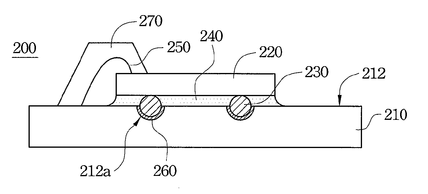
[0027] Refer to FIG. 2. FIG. 2 illustrates a cross-sectional view of a chip package in accordance with a first preferred embodiment of the present invention. A chip package 200 of the present embodiment comprises a package substrate 210, a chip 220, a plurality of spacers 230, an adhesive layer 240 and a plurality of wires 250. The package substrate 210 has a carrying surface 212, and the chip 220 is deposed on the carrying surface 212. The spacers 230 are formed between the chip 220 and the carrying surface 212 to maintain an interval between the chip 220 and the package substrate 210. The adhesive layer 240 is deposed between the chip 220 and the carrying surface 212 to encapsulate the spacers 230. In the embodiment, the chip 220 is electrically connected to the package substrate 210 through the wires 250 by, for example, wire bonding, and a material of the adhesive layer 240 is epoxy resin for example.
[0028] Referring to FIG. 2 again, the carrying surface 212 of the package subs...
second embodiment
[0039] Refer to FIG. 5. FIG. 5 illustrates a cross-sectional view of a chip package in accordance with a second preferred embodiment of the present invention. The differentiation between the second embodiment and the first embodiment is a carrying surface 312 of a package substrate 310 in the second embodiment does not include the indentations 212a and the metal layers 260 in the indentations 212a (as shown in FIG. 2), and the spacers 330 are not metal balls but protuberances on the carrying surface 312, and a material of the spacers 330 is green print, for example.
[0040] In regard to shape, the spacers 330 are in a shape of lump or bar, for example. When the spacers 330 are in the shape of a lump, the arrangement of the spacers 330 can have various modifications such as recited in the first embodiment, and the details are not given thereupon.
[0041] Refer to FIG. 6. FIG. 6 illustrates a top view of a portion of the chip package illustrated in FIG. 5, wherein the diagram illustrate...
PUM
 Abstract
Description
Claims
Application Information