Method for the manufacture of a strained silicon-on-insulator structure

a technology of strained silicon and on-insulator, which is applied in the direction of basic electric elements, electrical apparatus, and semiconductor devices, can solve the problems of inconvenient production of fully-depleted strained-semiconductor-on-insulator devices, inconvenient structure, and difficult to achieve the thickness required for fully-depleted silicon-on-insulator device fabrication

a technology of strained silicon and on-insulator, which is applied in the direction of basic electric elements, electrical apparatus, and semiconductor devices, can solve the problems of inconvenient production of fully-depleted strained-semiconductor-on-insulator devices, inconvenient structure, and difficult to achieve the thickness required for fully-depleted silicon-on-insulator device fabrication

US20070045738A1Inactive Publication Date: 2007-03-01MEMC ELECTONIC MATERIALS INC

Image

  • Method for the manufacture of a strained silicon-on-insulator structure
  • Method for the manufacture of a strained silicon-on-insulator structure
  • Method for the manufacture of a strained silicon-on-insulator structure

Examples


example

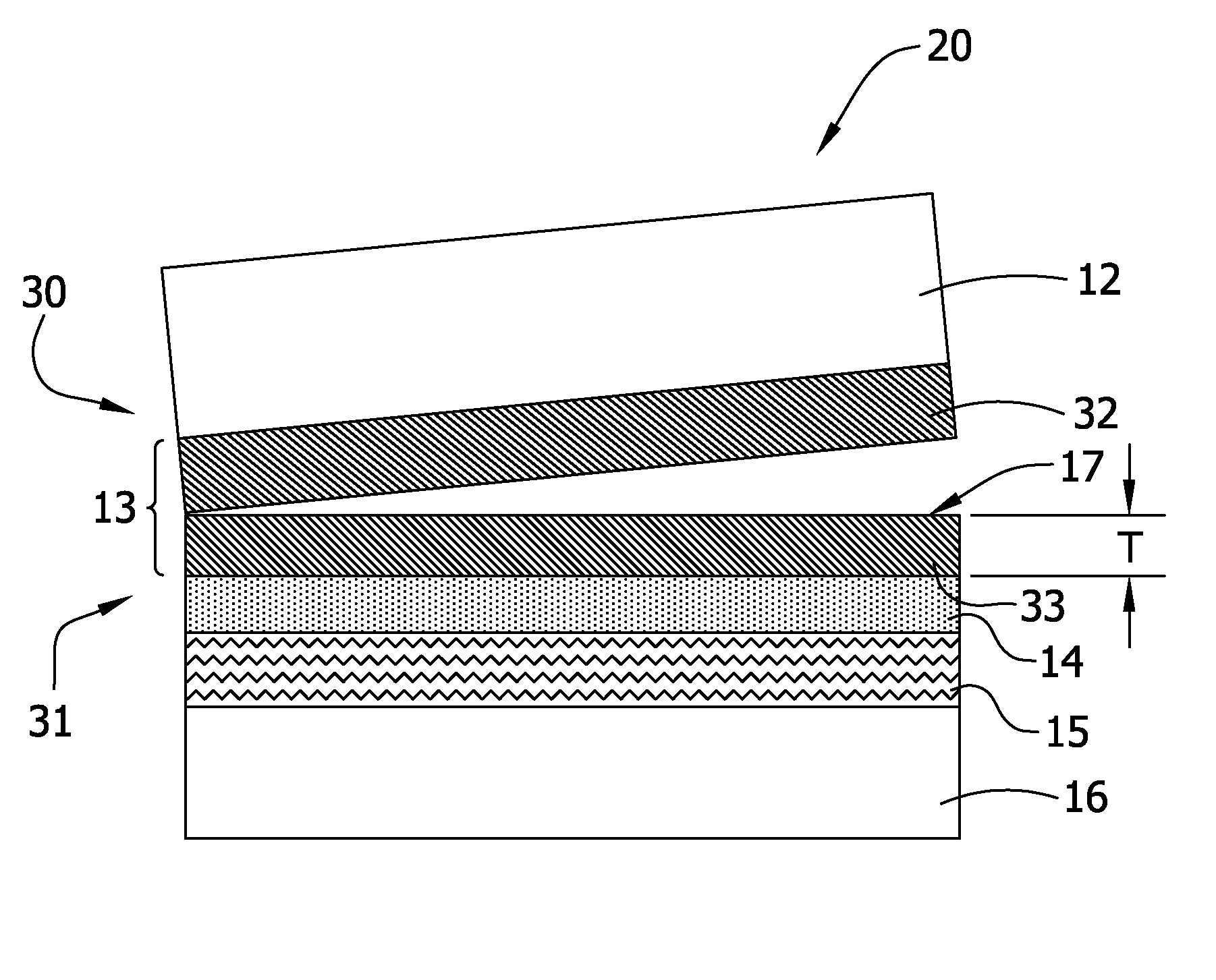
[0058] A crude SOI structure was prepared using common techniques in the art, such that, after separation, the resulting structure comprised the handle wafer, the SiO2 layer, the strained silicon layer thereon, and a residual relaxed SiGe layer on the strained silicon layer, the residual relaxed layer having a thickness of 120 nm. This structure was then exposed to NH4OH:H2O2:H2O etchant having a ratio of 1:2:50 for 240 min at about 65° C., while a megasonic treatment of about 1500 W was applied, in order to substantially remove the residual relaxed layer from the surface of the strained layer.

[0059] The resulting strained silicon surface was evaluated for RMS roughness, residual Ge concentration, and LPD concentration. The silicon surface showed an RMS roughness of about 0.8 nm using a 30 μm×30 μm field of view. Further, the residual Ge concentration was measured to be about 1.0×10¹⁰ Ge atoms / cm2. Finally, the LPD concentration was detected to be about 0.35 LPDs / cm2, while the dia...


PUM


Abstract

The present invention is directed to a strained silicon on insulator (SSOI) structure having improved surface characteristics, such as reduced roughness, low concentration of LPDs, and lower contamination, and a method for making such a structure.

Description

REFERENCE TO RELATED APPLICATIONS [0001] This application claims priority from U.S. provisional application Ser. No. 60 / 712,022 filed on Aug. 26, 2005, the entire disclosure of which is incorporated herein by reference.FIELD OF THE INVENTION [0002] The present invention relates generally to a strained silicon-on-insulator (SSOI) structure. More particularly, the present invention is directed to an SSOI structure wherein the strained silicon layer has improved surface properties. The present invention is further directed to a method for making such a structure. BACKGROUND OF THE INVENTION [0003] Silicon-on-insulator (SOI) structures generally comprise a handle wafer, a semiconductor device layer, and a dielectric insulating layer between the handle wafer and the device layer. By insulating the device layer from the handle wafer of the SOI structure, the device layer yields reduced leakage currents and lower capacitance. Strained silicon-on-insulator (SSOI) structures for semiconducto...

Claims


Application Information

Patent Timeline
01 Mar 2007
Publication
US20070045738A1
IPC
H01L27/12; H01L21/30
CPC
H01L21/76251; H01L27/1266; H01L29/7842; H01L21/76254; H01L21/762; H01L21/20; H01L27/12
Inventors
JONES, ANDREW M.; FEI, LU