Silicon-on-insulator chip with multiple crystal orientations

a technology of silicon-on-insulator chip and crystal orientation, which is applied in the direction of semiconductor devices, electrical devices, transistors, etc., can solve the problems of significant challenges and achieve the effect of enhancing the performance of n-channel and p-channel transistors

Inactive Publication Date: 2005-06-07
TAIWAN SEMICON MFG CO LTD
View PDF26 Cites 140 Cited by
  • Summary
  • Abstract
  • Description
  • Claims
  • Application Information

AI Technical Summary

Benefits of technology

[0013]The preferred embodiment of the present invention relates to a semiconductor device that includes active areas with different crystal orientations. This configuration is useful because the crystal plane orientation can be selected to enhance the performance of n-channel and p-channel transistors. For example, n-channel transistors can be formed in silicon regions with a (100) orientation and p-channel transistors can be formed in regions with a (110) orientation. In the preferred embodiment, the semiconductor device is a silicon-on-insulator device.

Problems solved by technology

Significant challenges are faced when transistors are scaled into the sub-100 nm regime.

Method used


Image

  • Silicon-on-insulator chip with multiple crystal orientations
  • Silicon-on-insulator chip with multiple crystal orientations
  • Silicon-on-insulator chip with multiple crystal orientations

Examples


first embodiment

[0041]The first embodiment method will now be described with respect to FIGS. 4a-4e. As shown in FIG. 4a, a silicon-on-insulator wafer 102 is provided where the crystalline silicon layer 130 has a first crystal orientation (h k l). Therefore, the surface of the silicon layer is of the (h k l) crystal orientation. Such a silicon-on-insulator 102 wafer may be formed by a wafer bonding and wafer separation technique, or by an oxygen implantation (SIMOX) technique, as examples.

[0042]Selected portions 134 of the silicon layer 130 are amorphosized, i.e., transformed to the amorphous state. This transformation can be performed by masking the wafer 102, opening the mask 132 at the selected portions 134 of the silicon layer 130 to be amorphosized, and implanting ions 136 into the selected portions 134 of the silicon layer 130 to create an amorphous region as shown in FIG. 4b. The ion implantation can be done by conventional ion implantation techniques such as beam-line ion implantation or pl...

second embodiment

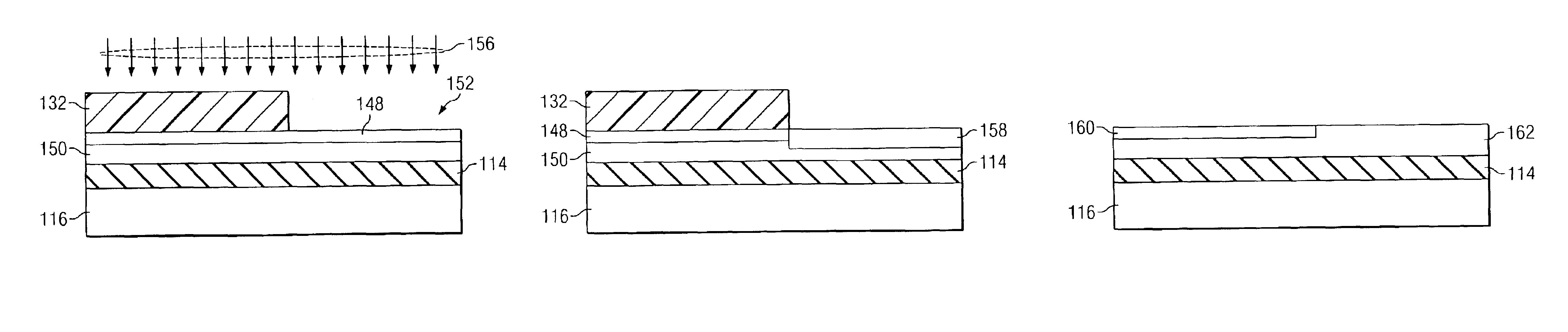
[0047]FIGS. 5a-5f show a second embodiment method of the present invention. A silicon-on-insulator wafer 104 is provided as shown in FIG. 5a. The silicon layer in FIG. 5a includes at least two layers 148 and 150 of silicon with different crystal orientations. As shown in FIG. 5, a topmost silicon layer 148 with the (h k l) crystal orientation overlies a silicon layer 150 with the (h′ k′ l′) crystal orientation. The thickness of the topmost silicon layer 148 may vary from about 10 angstroms to about 500 angstroms, but is preferably less than about 50 angstroms. The thickness of the silicon layer 150 maybe in the range of about 10 to about 500 angstrom and is once again less than about 50 angstroms.

[0048]In one example, the topmost silicon layer 148 can be formed by a layer transfer technique, which comprises of a wafer bonding process and a wafer separation process. For example, we may begin with a silicon-on-insulator target wafer which comprises of a (100)-oriented silicon layer ov...

fifth embodiment

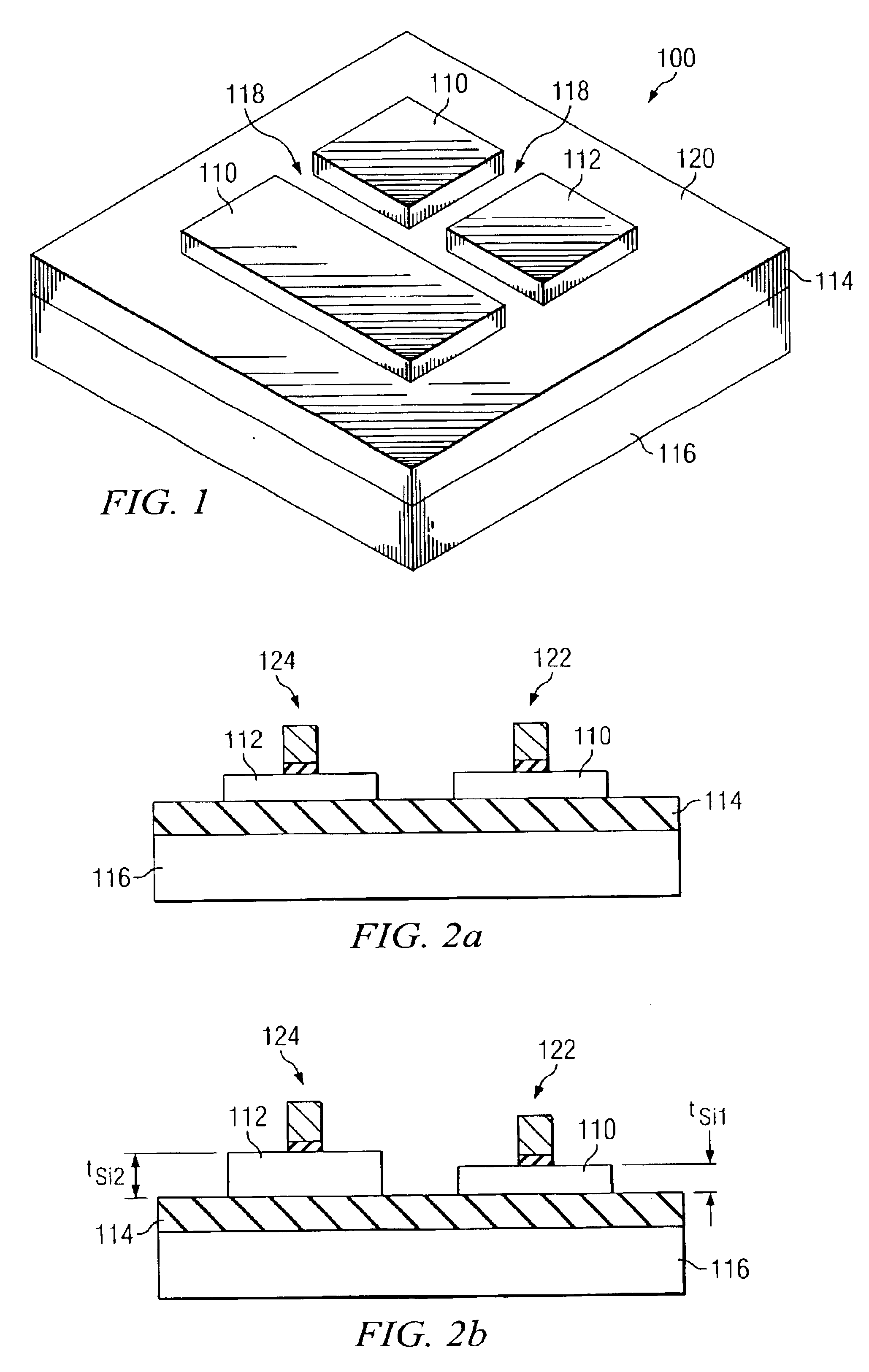
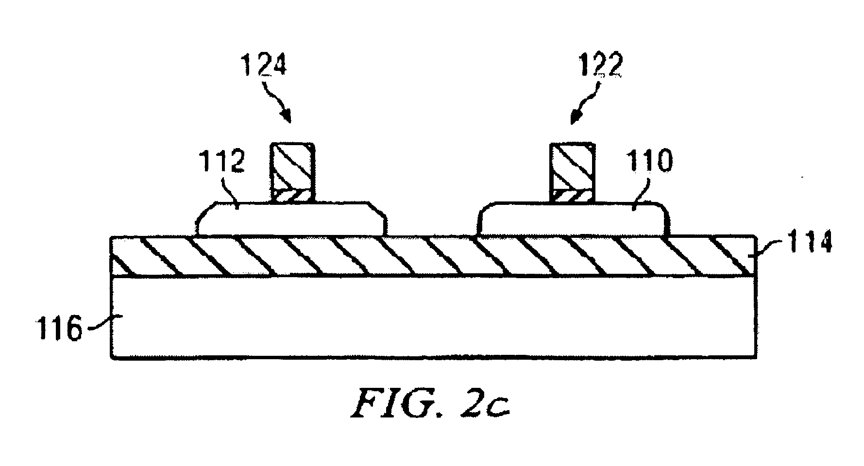
[0057]Referring now to FIG. 8a-8c, a fifth embodiment method is discussed. A silicon-on-insulator wafer 106 is provided where the crystalline silicon layer has a first crystal orientation (h k l), as shown in FIG. 8a. Referring to FIG. 8b, selected portions of the silicon layer 130 are etched to expose the crystalline surface 138 insulator 114. This can be done by masking the wafer with a mask 132, opening the mask 132 at the selected portions of the silicon layer 130 to be etched, and etching the selected portions of the silicon layer 130 by dry or wet etching.

[0058]Epitaxy is then performed to grown a silicon layer 164 with a (h′ k′ l′) crystal orientation on the exposed crystalline insulator surface. The epitaxy step can be performed before the mask 132 is removed, as shown in FIG. 8c, or after the mask 132 is removed. This step will result in a first region 166 with a (h k l) crystal orientation and a second silicon region 164 with a (h′ k′ l′) crystal orientation. Silicon islan...


PUM


Abstract

A silicon-on-insulator chip includes an insulator layer, typically formed over a substrate. A first silicon island with a surface of a first crystal orientation overlies the insulator layer and a second silicon island with a surface of a second crystal orientation also overlies the insulator layer. In one embodiment, the silicon-on-insulator chip also includes a first transistor of a first conduction type formed on the first silicon island, and a second transistor of a second conduction type formed on the second silicon island. For example, the first crystal orientation can be (110) while the first transistor is a p-channel transistor, and the second crystal orientation can be (100) while the second transistor is an n-channel transistor.

Description

CROSS-REFERENCE TO RELATED APPLICATIONS[0001]The following U.S. patents and / or commonly assigned patent applications are hereby incorporated herein by reference:[0002]Pat. orSer. No.Filing DateIssue Date 10 / 379,873Mar. 5, 200310 / 384,859Mar. 10, 2003TECHNICAL FIELD[0003]The present invention relates generally to semiconductor devices, and, in particular embodiments, to a silicon-on-insulator chip including silicon islands with multiple crystal plane orientations to enhance the performances of n-channel and p-channel transistors and several methods for the formation of such a silicon-on-insulator chip.BACKGROUND[0004]Complementary metal-oxide-semiconductor (CMOS) technology is the dominant semiconductor technology used for the manufacture of ultra-large scale integrated (ULSI) circuits today. Conventional CMOS technology employs (100) silicon wafer as the starting material for volume production. Such silicon wafers have a surface that is (100) oriented, i.e., the normal to the silicon...

Claims


Application Information

Patent Timeline
Patent Type & Authority Patents(United States)
IPC IPC(8): H01L21/70H01L21/84H01L27/12
CPCH01L27/1203H01L21/84
Inventor YEO, YEE-CHIAYANG, FU-LIANG
Owner TAIWAN SEMICON MFG CO LTD
Why Eureka
Try Eureka