
SOI DRAM having P-doped poly gate for a memory pass transistor

a memory pass transistor and poly gate technology, applied in transistors, semiconductor devices, electrical equipment, etc., can solve the problems of high source/drain resistance of fully depleted transistors, cost, yield, and difficulty in using soi for dram

Inactive Publication Date: 2004-03-09
TEXAS INSTR INC
View PDF8 Cites 142 Cited by
  • Summary
  • Abstract
  • Description
  • Claims
  • Application Information

AI Technical Summary

Problems solved by technology

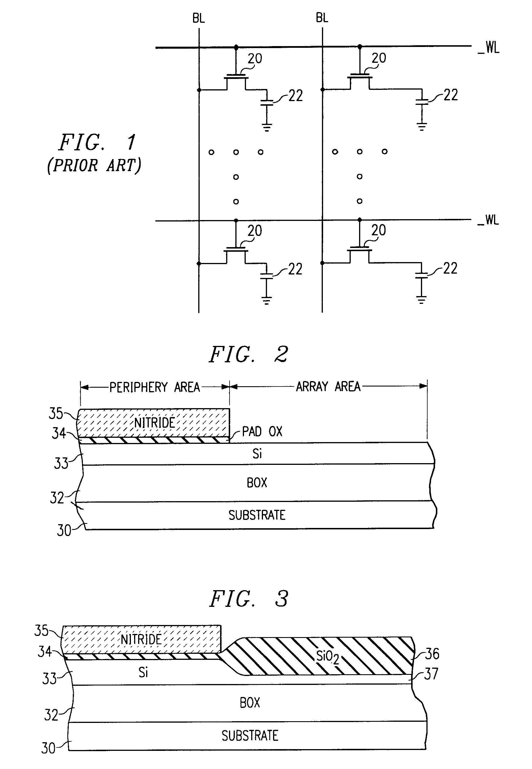
There are also potential difficulties in using SOI for DRAM.
These include cost, yield, and floating body effects.
In addition to the difficulty of selecting desirable threshold voltage, fully depleted transistors suffer from higher source / drain resistance because of the thinner silicon film.
The fully depleted transistor also has reduced floating body effects that can increase leakage in pass transistors and lead to variation of threshold voltages which would be deleterious to sense amplifiers.
However, the threshold voltage of a fully depleted n-channel SOI transistor with n-poly gate is too low for DRAM pass transistor application.

Method used


Image

  • SOI DRAM having P-doped poly gate for a memory pass transistor
  • SOI DRAM having P-doped poly gate for a memory pass transistor
  • SOI DRAM having P-doped poly gate for a memory pass transistor

Examples


second example

Uniform thickness for Silicon channel: 60 mm

Single gate material: P+polysilicon

(1) Pass transistors: fully depleted n-channel transistors with 1E17 p type doping in channel. (Vt=.about.1.2V)

(2) n-channel periphery transistors: fully depleted transistors with 3E16 n type doping in channel. (Accumulation mode, Vt=.about.0.5V)

(3) p-channel periphery transistors: partially depleted transistors with 6E17 n type doping in channel. (Vt=.about.-0.5V)

third example

Uniform thickness for Silicon channel: 60 mm

Single gate material: p+polysilicon

(1) Pass transistors: fully depleted n-channel transistors with 1E16 n type doping in channel. (Accumulation mode, Vt=.about.0.8V)

(2) n-channel periphery transistors: fully depleted transistors with 3E16 n type doping in channel. (Accumulation mode, Vt=.about.-0.5V)

(3) p-channel periphery transistors: partially depleted transistors with 6E17 n type doping in channel. (Vt=.about.-0.5V)

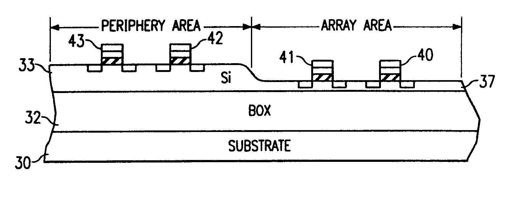
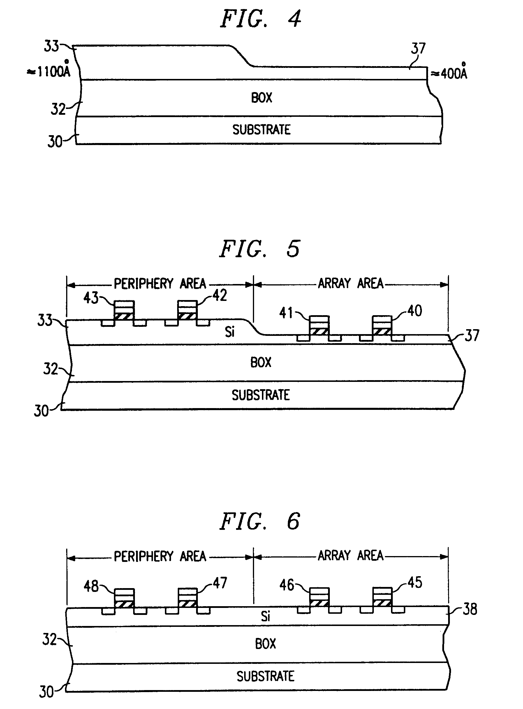
As stated above, it is possible to have fully depleted pass transistors in the array and partially depleted logic transistors in the periphery using different silicon film thicknesses. Another option is to use different gate materials. An example of this is as follows:

fourth example

Uniform thickness for Silicon channel: 60 nm

(1) Pass transistors: fully depleted p-channel transistors having n-doped poly gates with 1E17 n type doping in channel. (Vt=.about.-1.2V)

(2) n-channel periphery transistors: partially depleted transistors having n-doped poly gates with 6E17 p type doping in channel. (Vt=.about.0.5V)

(3) p-channel periphery transistors: partially depleted transistors having p-doped poly gates with 6E17 n type doping in channel. (Vt=.about.-0.5V)

It should be recognized that the above examples were given knowing that the devices can be optimized with channel profiling and source / drain engineering. Therefore, the invention is not intended to be limited to the above examples.

The p-channel pass transistor has an advantage relative to the n-channel pass for SOI because of the lower parasitic bipolar gain for a p-n-p structure vs a n-p-n structure. Also, if opposite gate doping is used (n-poly for p-channel or p-poly for n-channel) the n-poly gate of the p-channel...


PUM


Abstract

An integrated circuit including a DRAM is disclosed, wherein the DRAM includes a memory array including a plurality of pass gate transistors and a plurality of memory elements. The pass gate transistors include a gate material selected to provide a substantially near mid-gap work function or greater. The DRAM also includes a peripheral area including a plurality of logic transistors. In a preferred embodiment the pass gate transistors are silicon-on-insulator transistors.

Description

1. Field of the InventionThis invention relates to a the design of DRAMs using Silicon on Insulator (SOI) technology and more particularly to the design of fully depleted memory pass transistors in the DRAM in combination with a P-doped polysilicon gate.2. Description of the Prior ArtSOI is good for DRAM for several reasons. One reason is that SOI has lower collection volume for charge generated by an alpha particle or a cosmic ray. Such charge can upset the memory cell, so the smaller collection volume of SOI is desirable. SOI also reduces the capacitance on the bit line so less charge is needed to generate an equivalent signal on the bit line relative to bulk DRAM. Also reduced junction area in the memory cell should give lower leakage which translates to longer retention time. All these features, lower collection volume, lower leakage and lower capacitance, are advantages of SOI.There are also potential difficulties in using SOI for DRAM. These include cost, yield, and floating b...

Claims


Application Information

Patent Timeline
Patent Type & Authority Patents(United States)
IPC IPC(8): H01L27/12H01L21/70H01L21/84H01L21/8242H01L27/02H01L27/108
CPCH01L27/10894H01L27/10897H01L27/1203H01L21/84H01L27/10873H01L27/0218H10B12/05H10B12/50H10B12/09
Inventor HOUSTON, THEODORE W.
Owner TEXAS INSTR INC
Learn More