

SCR devices in silicon-on-insulator CMOS process for on-chip ESD protection
a technology of silicon-on-insulator and cmos, applied in the direction of semiconductor devices, semiconductor/solid-state device details, electrical apparatus, etc., can solve the problems of not being able to protect gate oxides, being susceptible to electrostatic discharge events, and being triggered by substrate noise accidentally
- Summary
- Abstract
- Description
- Claims
- Application Information
AI Technical Summary
Problems solved by technology
Method used
Image

Examples
Embodiment Construction
[0001] 1. Field of the Invention
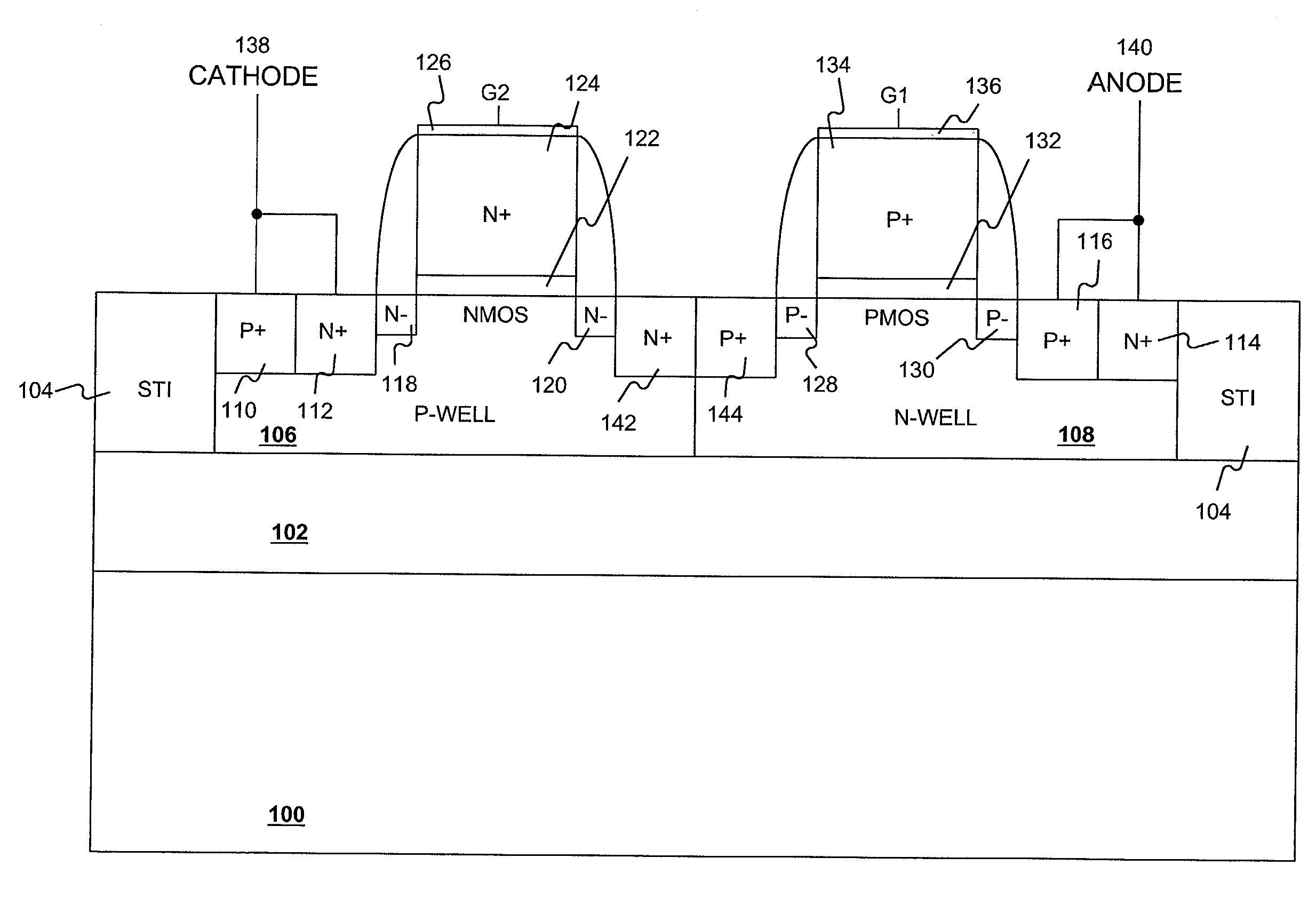
[0002] This invention pertains in general to a semiconductor device and, more particularly, to an electrostatic discharge protection circuit incorporating a silicon controlled rectifier in a silicon-on-insulator semiconductor device.
[0003] 2. Background of the Invention
[0004] Recent advances in integrated circuits have included further development of a silicon-on-insulator (SOI) technology. An SOI technology uses an insulating substrate to improve process characteristics such as speed and latch-up susceptibility. There are two types of SOI processes, fully-depleted and partially-depleted.
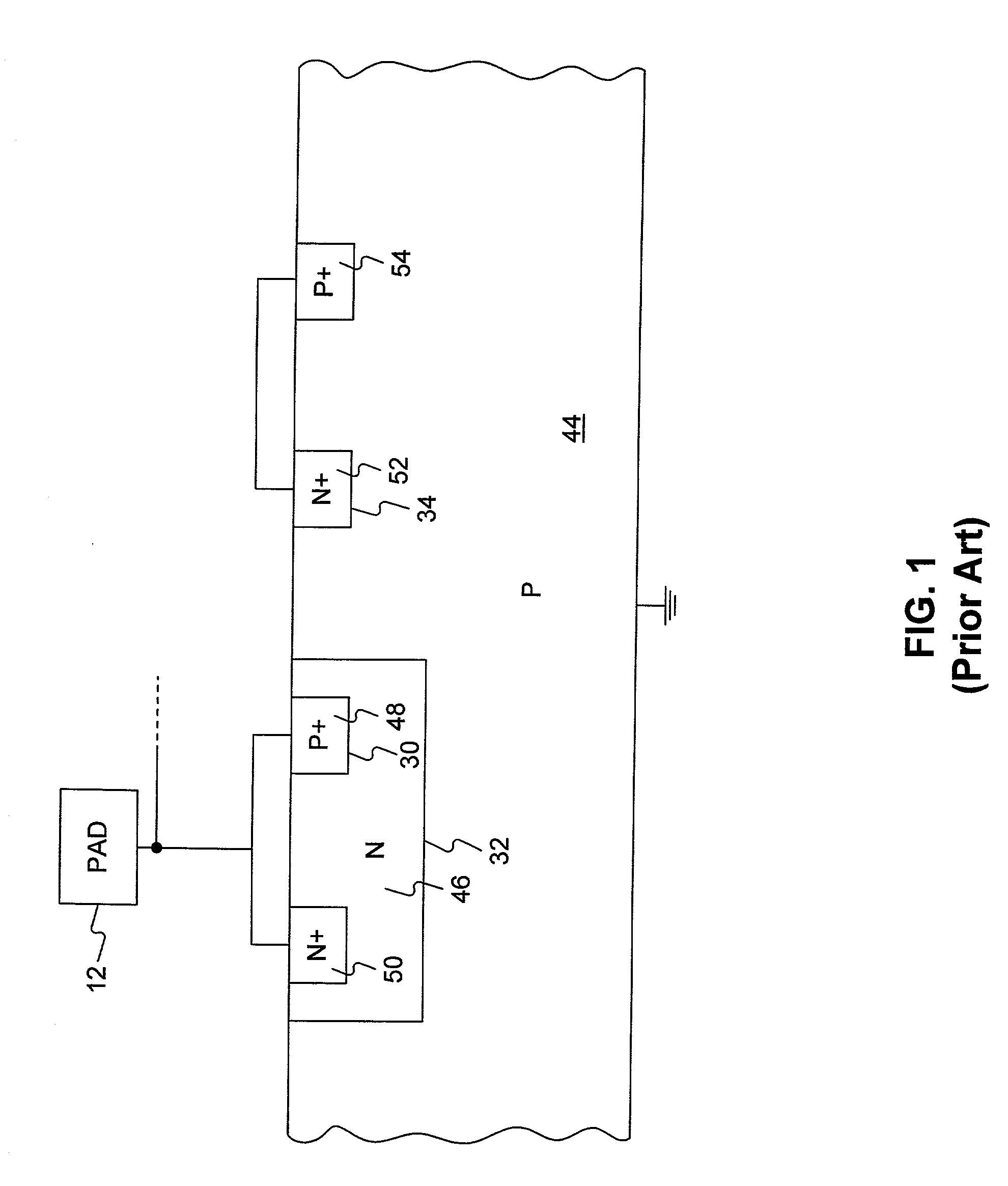
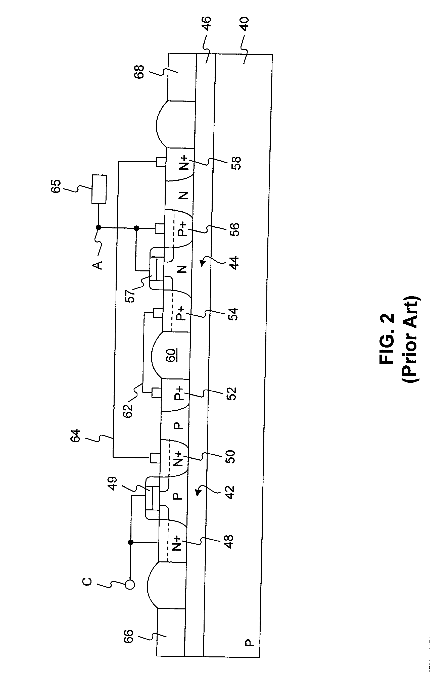
[0005] In an SOI complementary metal-oxide semiconductor (CMOS) technology, an independent and isolated n-type metal-oxide semiconductor (NMOS) transistor may be provided next to a p-type MOS (PMOS) transistor, and vice versa, because the NMOS and PMOS transistors are electrically isolated from each other and from the underlying silicon substrate. The main advantage o...
PUM
| Property | Measurement | Unit |
|---|---|---|
| voltage-holding | aaaaa | aaaaa |
| switching voltage | aaaaa | aaaaa |
| semiconductor | aaaaa | aaaaa |
Abstract
Description
Claims
Application Information