Electrically erasable programmable read-only memory cell transistor and related method

Inactive Publication Date: 2007-03-01
SAMSUNG ELECTRONICS CO LTD
View PDF19 Cites 21 Cited by
  • Summary
  • Abstract
  • Description
  • Claims
  • Application Information

AI Technical Summary

Benefits of technology

[0018] Therefore, embodiments of the invention provide an electrically erasable programmable read-only memory (EEPROM) cell transistor having an increased data storage capacity of 2 or more bits of data, wherein the EEPROM cell transistor comprises a floating gate elect

Problems solved by technology

However, in portable computational devices, such as PDA's and notebook computers, the hard disk apparatus occupies a great deal of available space.
However, the conventional EEPROM cell transistor of FIG. 1 is not able to store more than 1 bit of data in accordance with presence of stored charge on floating gate electrode 14.
Thus, the storage capacity of the conventional EEPROM cell transistor of FIG. 1 is less than a cell transistor capable of

Method used


Image

  • Electrically erasable programmable read-only memory cell transistor and related method
  • Electrically erasable programmable read-only memory cell transistor and related method
  • Electrically erasable programmable read-only memory cell transistor and related method

Examples


Embodiment Construction

[0027] As used herein, when a first element is said to be “on” a second element, the first element may be directly on the second element, or intervening elements may be present.

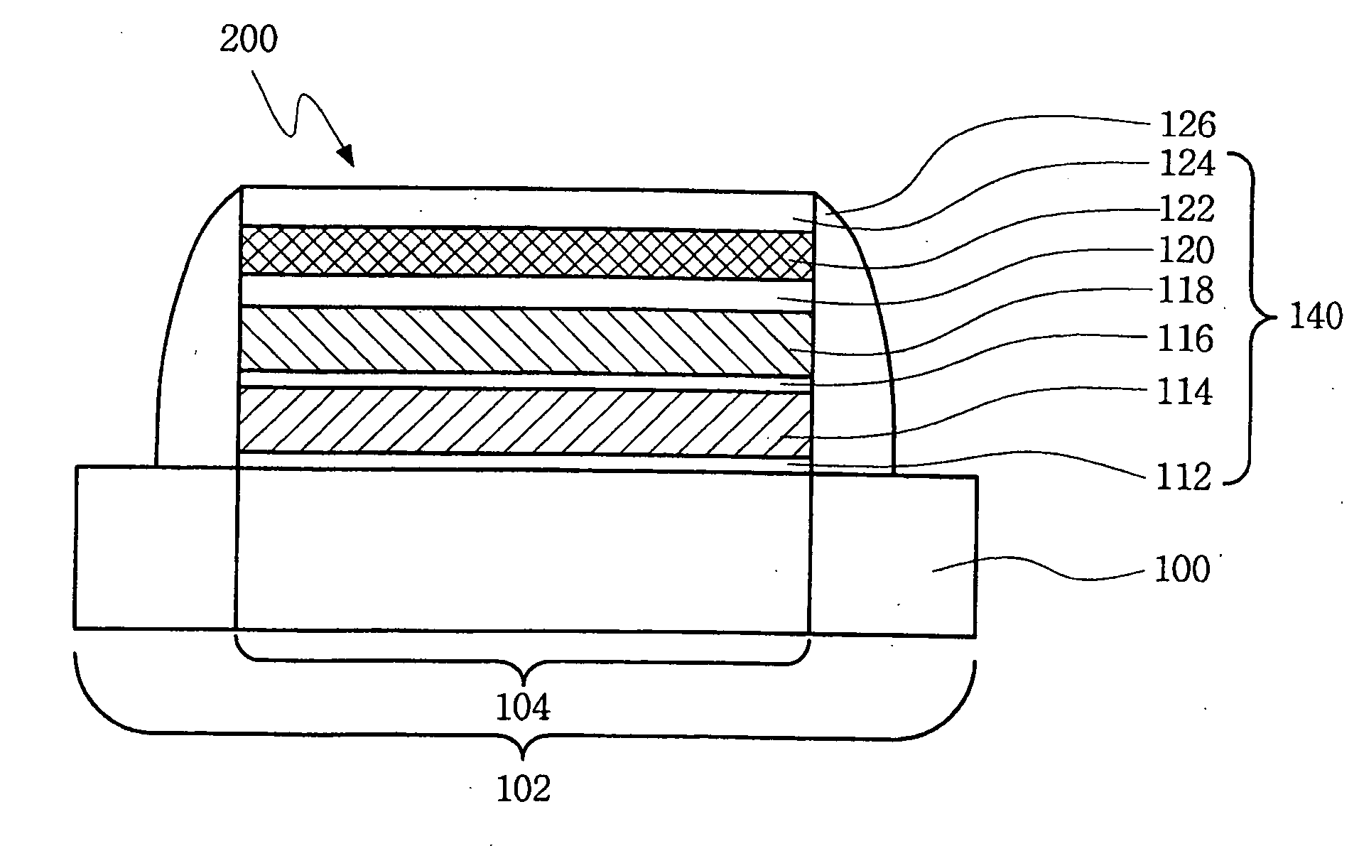
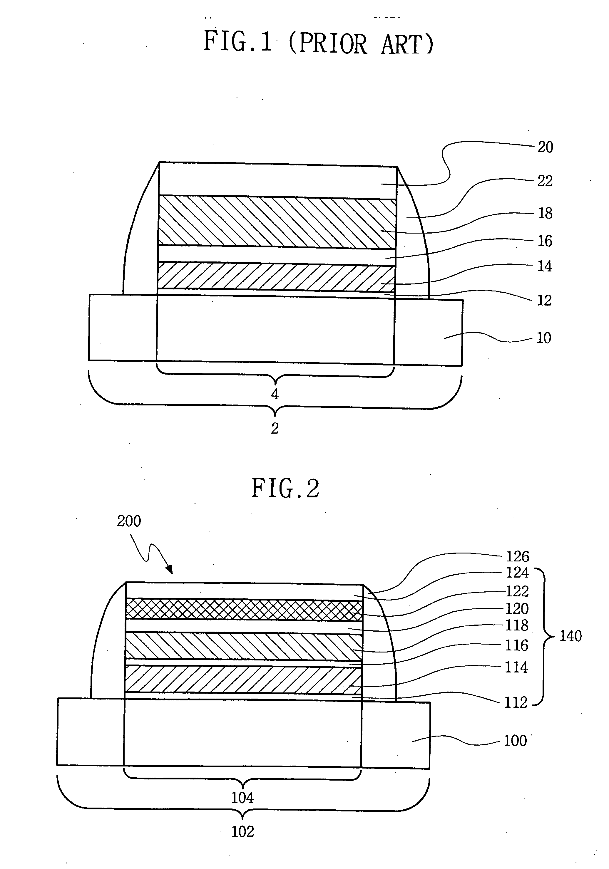
[0028]FIG. 2 is a cross-sectional view illustrating the structure of an electrically erasable programmable read-only memory (EEPROM) cell transistor in accordance with an embodiment of the invention.

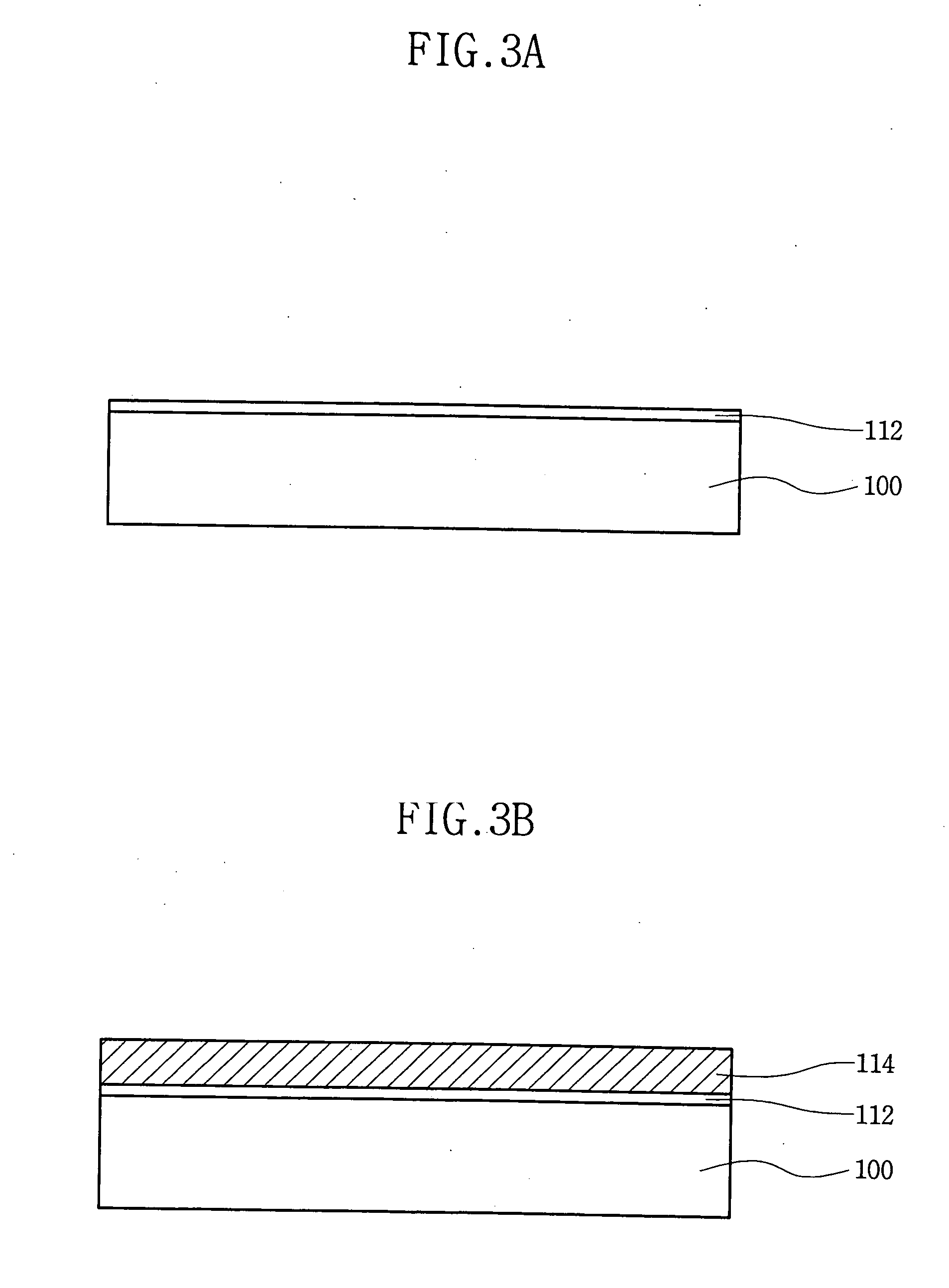
[0029] As illustrated in FIG. 2, an EEPROM cell transistor 200 comprises a semiconductor substrate 100 having an active region 102 defined by an electrically insulated isolation layer (not shown) or an electrically insulated field oxide layer (not shown). Also, active region 102 comprises a channel region 104. EEPROM cell transistor 200 further comprises a first tunnel oxide layer 112 having a predetermined thickness and formed on semiconductor substrate 100, a first floating gate electrode 114 formed from a phase changeable material (e.g., GeSeTe) and formed on first tunnel oxide layer 112, and a second tunnel ...


PUM


Abstract

An electrically erasable programmable read-only memory (EEPROM) cell transistor and a method of fabricating the EEPROM cell transistor are provided. The EEPROM cell transistor comprises a semiconductor substrate; a first tunnel oxide layer formed on the semiconductor substrate; and a first floating gate electrode formed on the first tunnel oxide layer and adapted to store charge that tunnels through the first tunnel oxide layer. The EEPROM cell transistor further comprises a second tunnel oxide layer formed on the first floating gate electrode; a second floating gate electrode formed on the second tunnel oxide layer and adapted to store charge that tunnels from the first floating gate electrode through the second tunnel oxide layer, wherein the second floating gate electrode is formed from a phase changeable material; a gate insulating layer formed on the second floating gate electrode; and a control gate electrode formed on the gate insulating layer.

Description

BACKGROUND OF THE INVENTION [0001] 1. Field of the Invention [0002] Embodiments of the invention relate to a nonvolatile semiconductor memory device and a method for fabricating the nonvolatile semiconductor memory device. In particular, embodiments of the invention relate to an electrically erasable programmable read-only memory (EEPROM) cell transistor comprising two floating gate electrodes, wherein at least one of the floating gate electrodes is formed from a phase changeable material, and a method of fabricating the EEPROM cell transistor. [0003] This application claims priority to Korean Patent Application No. 10-2005-0078166, filed Aug. 25, 2005, the subject matter of which is hereby incorporated by reference in its entirety. [0004] 2. Description of Related Art [0005] There is a continuing commercial demand for highly-integrated electrically erasable programmable read-only memory (EEPROM) devices adapted for use within various host devices such as computers, telecommunicatio...

Claims


Application Information

Patent Timeline
IPC IPC(8): G11C16/04
CPCG11C13/0004H01L21/28273G11C2213/53G11C16/0458H01L29/40114H10B41/35
Inventor KIM, JUN-SEUCK
Owner SAMSUNG ELECTRONICS CO LTD
Why Eureka
Try Eureka