
Overlay target for polarized light lithography

Inactive Publication Date: 2007-03-01
INFINEON TECH AG
View PDF1 Cites 11 Cited by
  • Summary
  • Abstract
  • Description
  • Claims
  • Application Information

AI Technical Summary

Benefits of technology

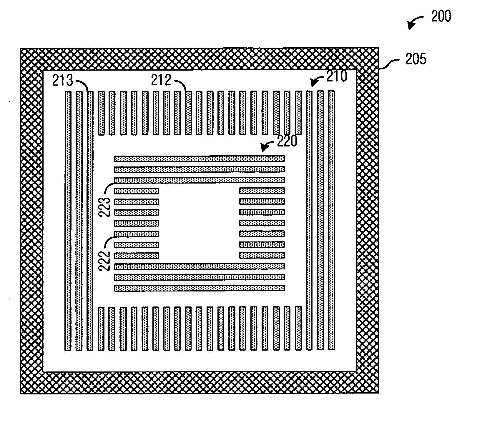
[0012] An advantage of a preferred embodiment of the present invention is that the overlay target can be used to measure layer misalignments due to mechanical shifts, lens magnification errors, and lens aberration errors.
[0013] A further advantage of a preferred embodiment of the present invention is that the overlay target can be used with a single reference layer. This can simplify overlay target design and use. Furthermore, the use of a single reference layer can result in more accurate layer alignment since layer misalignment is not allowed to build up through successive layers.
[0014] Yet another advantage of a preferred embodiment of the present invention is that the overlay target can be used with layers formed with both horizontal and vertical polarized light. This can simplify overlay target design and use since a single overlay target can be used, rather than requiring multiple overlay target designs.

Problems solved by technology

Misalignment of the layers can reduce the performance of the integrated circuitry if the misalignment is small (due to improper device geometries) and inoperable integrated circuitry if the misalignment is large (due to formation of improper electrical connections).
Misalignment of the layers can arise when a photomask is used to pattern a layer and the photomask is not lined up properly with previously created layers on the semiconductor wafer.
Misalignment can be due to mechanical shift errors, optical lens magnification errors, optical lens aberration errors, and so forth.
Mechanical shift errors can be the result of shifts in the semiconductor wafer and / or the photomask during processing and optical lens magnification errors can be a result of magnification mismatches between different layers of the semiconductor wafer.
Optical lens aberration errors can be the result of non-ideal characteristics of an optical lens being used, wherein light passing through the lens behaves differently depending upon the portion of the lens the light is passing through.
One disadvantage of the prior art is that the overlay targets can be used to detect mechanical shift errors and lens magnification errors.
However, lens aberrations can also result in significant misalignment errors and the prior art overlay targets do not adequately capture lens aberration errors.
A second disadvantage of the prior art is that the overlay targets do not exploit the advantages of using polarized light.
Yet another disadvantage of the prior art is that the overlay targets typically comprise the photoresist layer and a layer immediately beneath it.
The use of adjacent layers can permit a sequential build-up of misalignment that, while between the adjacent layers is within specifications, can lead to an overall misalignment that exceeds specifications.

Method used


Image

  • Overlay target for polarized light lithography
  • Overlay target for polarized light lithography
  • Overlay target for polarized light lithography

Examples


Embodiment Construction

[0022] The making and using of the presently preferred embodiments are discussed in detail below. It should be appreciated, however, that the present invention provides many applicable inventive concepts that can be embodied in a wide variety of specific contexts. The specific embodiments discussed are merely illustrative of specific ways to make and use the invention, and do not limit the scope of the invention.

[0023] The present invention will be described with respect to preferred embodiments in a specific context, namely semiconductor fabrication using polarized light lithography. The invention may also be applied, however, to other semiconductor fabrications techniques involving lithography, including those using non-polarized light.

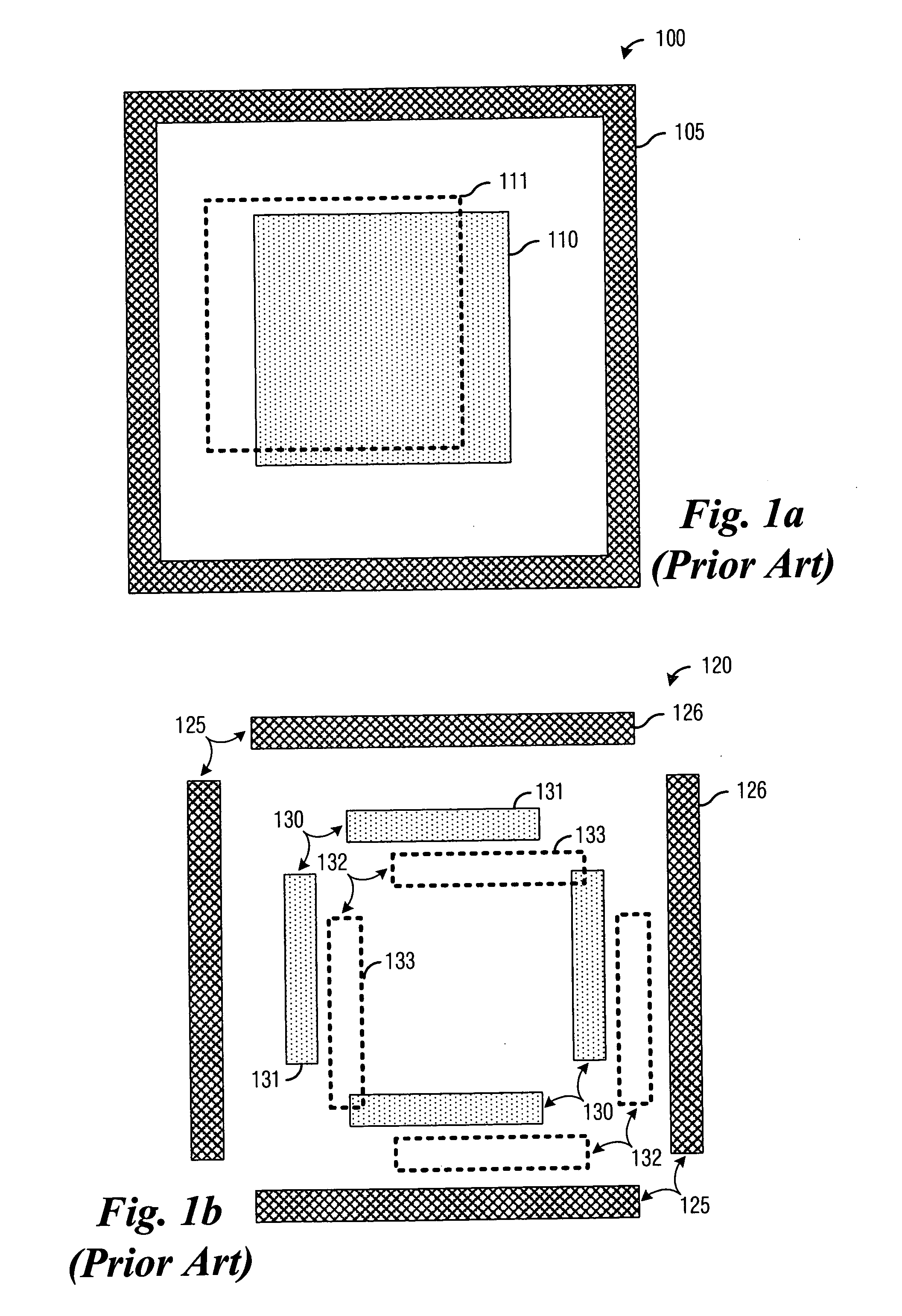
[0024] With reference now to FIGS. 1a and 1b, there are shown diagrams illustrating exemplary prior art overlay targets. The diagram shown in FIG. 1a illustrates a first prior art overlay target 100. The first overlay target 100 comprises a frame ...


PUM


Abstract

A target and method for use in polarized light lithography. A preferred embodiment comprises a first structure located on a reference layer, wherein the first structure is visible through a second layer, and a second structure located on the second layer, wherein the second structure is formed from a photomask containing a plurality of sub-structures oriented in a first orientation, wherein a polarized light is used to pattern the second structure onto the second layer, and wherein a polarization of the polarized light is the same as the orientation of the plurality of sub-structures. The position, size, and shape of the second structure is dependent upon a polarity of the polarized light, permitting a single design for an overlay target to be used with different polarities of polarized light.

Description

TECHNICAL FIELD [0001] The present invention relates generally to integrated circuit wafer fabrication, and more particularly to an overlay target and a method for use in polarized light lithography. BACKGROUND [0002] The fabrication of integrated circuits on semiconductor wafers typically involves the creation of multiple, successive layers of materials, such as insulators, conductors, semiconductors, and so forth, on the semiconductor wafers. Each of the layers is normally formed by applying a photoresist layer over previously formed layers and then the photoresist layer is patterned. Portions of the photoresist layer not exposed during the patterning can be washed off and the layer can be formed using one of many desired techniques. When completed properly, the multiple layers combine to form functional integrated circuits. The alignment of the individual layers is crucial to creating properly formed structures in the semiconductor wafer. Misalignment of the layers can reduce the...

Claims


Application Information

Patent Timeline
IPC IPC(8): G03F1/00
CPCG03F7/70566G03F7/70683G03F7/70633
Inventor MAROKKEY, SAJAN
Owner INFINEON TECH AG
Learn More