Capacitor over red pixel

a capacitor and red pixel technology, applied in the field of signal processing system, can solve the problem of less photo-conversion device availability, and achieve the effect of increasing the size of the photosensitive region of the pixel, filling factor and charge storage capacity

Active Publication Date: 2007-03-08
APTINA IMAGING CORP
View PDF20 Cites 64 Cited by
  • Summary
  • Abstract
  • Description
  • Claims
  • Application Information

AI Technical Summary

Benefits of technology

[0010] In another aspect, a capacitor is provided over one red pixel and the capacitor and read out circuit of that pixel is shared with other different pixels. Since red light is absorbed deeper in the silicon of an array, the capacitor over the photosensitive region of a red pixel does not significantly effect photons received by the red pixel. With neighboring non-red pixels sharing the capacitor and the readout circuit of the red pixel, the size of the photosensitive regions of the pixels can be increased. Accordingly, both fill factor and charge storage capacity are increased.

Problems solved by technology

There is a tradeoff of space: the greater space consumed by capacitors in an array the less available for the photo-conversion devices 23.

Method used


Image

  • Capacitor over red pixel
  • Capacitor over red pixel
  • Capacitor over red pixel

Examples


Embodiment Construction

[0021] In the following detailed description, reference is made to the accompanying drawings, which form a part hereof, and in which is shown by way of illustration specific exemplary embodiments of the invention. These embodiments are described in sufficient detail to enable those of ordinary skill in the art to make and use the invention, and it is to be understood that structural, logical or other changes may be made to the specific embodiments disclosed without departing from the spirit and scope of the present invention.

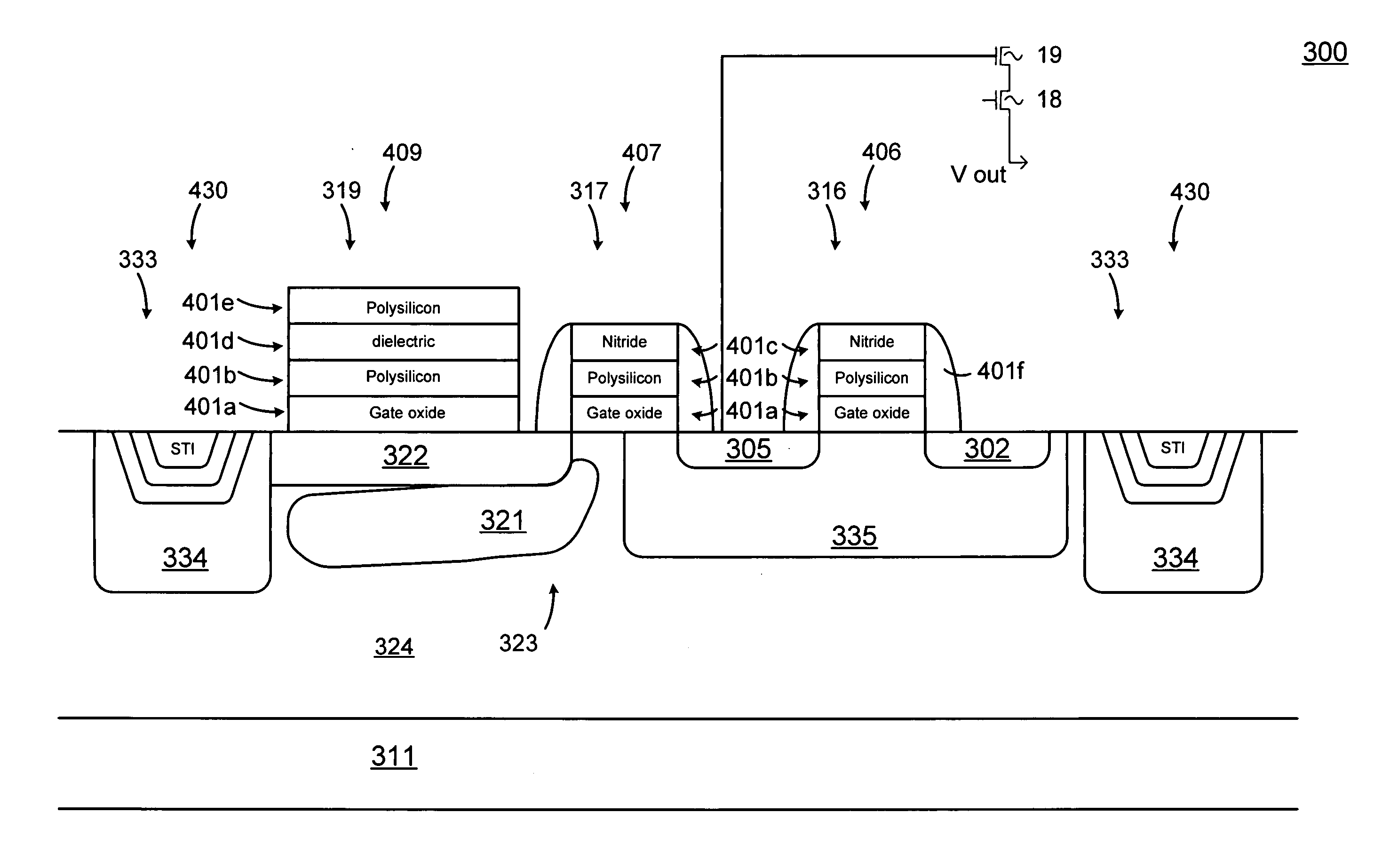
[0022]FIG. 4 is a cross-sectional view of a portion of pixel 300 according to an exemplary embodiment of the invention. The pixel 300 is similar to the pixel 10 depicted in FIGS. 2-3, except that the pixel 300 includes a capacitor 319 located above the photo-conversion device 323. In the exemplary embodiment, the pixel 300 is a red pixel, e.g., a pixel that receives red light in the form of photons and converts the photons to an electrical charge. A red pixel i...


PUM


Abstract

A red pixel having a capacitor formed over the photo-conversion region of the pixel. The capacitor can be used by other pixels as a common capacitor. The capacitor is coupled to floating diffusion region shared by a plurality of pixels. The plurality of pixels also share readout circuitry.

Description

[0001] The invention relates generally to semiconductor imaging devices and in particular to an imager having an array of pixel cells and circuitry for the cells which includes a capacitor. BACKGROUND OF THE INVENTION [0002] There is a current interest in CMOS active pixel imagers for use as low cost imaging devices. FIG. 1 shows a signal processing system 100 that includes a CMOS active pixel sensor (“APS”) pixel array 230 and a controller 232 that provides timing and control signals to enable the reading out of signals stored in the pixels in a manner commonly known to those skilled in the art. Exemplary arrays have dimensions of M×N pixels, with the size of the array 230 depending on a particular application. The imager pixels are readout a row at a time using a column parallel readout architecture. The controller 232 selects a particular row of pixels in the array 230 by controlling the operation of row addressing circuit 234 and row drivers 240. Charge signals stored in the sel...

Claims


Application Information

Patent Timeline
Patent Type & Authority Applications(United States)
IPC IPC(8): H01L31/06
CPCH01L27/14603H01L27/14609H01L27/14641H01L27/14683H04N5/335H01L27/14645H04N25/00H01L27/146
Inventor MCKEE, JEFFREY A.
Owner APTINA IMAGING CORP
Why Eureka
Try Eureka