Flat panel display device and method of correcting bonding misalignment of driver IC and flat panel display

a flat panel display and driver technology, applied in the direction of discharge tube luminescnet screens, discharge tubes/lamp details, instruments, etc., can solve the problems of reducing the yield after thermal pressing process, increasing the cost of lcd panels, and worse display quality of lcd panels, so as to avoid the failure of bonding and increase the yield

Inactive Publication Date: 2007-03-08
CHUNGHWA PICTURE TUBES LTD
View PDF3 Cites 24 Cited by
  • Summary
  • Abstract
  • Description
  • Claims
  • Application Information

AI Technical Summary

Benefits of technology

[0011] The present invention is also directed to a method of correcting bonding misalignment of a flat display panel and driver IC after the misalignment of the bonding between bumps and alignment mark is being identified to increase the yield of the thermal pressing process of the chip on glass (COG) method and to improve the display quality.
[0014] Accordingly, in the present invention, since a layout of the alignment mark is disposed around the pattern of the substrate, therefore the misalignment of the bonding between the driver IC and the liquid crystal display panel can be measured. Therefore, in the preceeding process, when the bonding of the driver IC and the liquid crystal display panel is performed, the identification of misalignment may be performed to optimize and correct the process tool and apparatus to avoid the failure of the bonding and to increase the yield.

Problems solved by technology

Therefore, the yield after the thermal pressing process is reduced, and thus the cost of the LCD panel is increased.
Therefore, the display quality of the LCD panel is worse due to the influence of the unexpected impedance to the electrical signal transmission caused due to the bonding misalignment.
Therefore, it is not practical to rework the failed bonded display panel.
Therefore, the cost of the LCD panel is highly dependent on the yield of the thermal pressing process of the chip on glass (COG) bonding method.

Method used


Image

  • Flat panel display device and method of correcting bonding misalignment of driver IC and flat panel display
  • Flat panel display device and method of correcting bonding misalignment of driver IC and flat panel display
  • Flat panel display device and method of correcting bonding misalignment of driver IC and flat panel display

Examples


Embodiment Construction

[0024] The present invention now will be described more fully hereinafter with reference to the accompanying drawings, in which embodiments of the invention are shown. This invention may, however, be embodied in many different forms and should not be construed as limited to the embodiments set forth herein; rather, these embodiments are provided so that this disclosure will be thorough and complete, and will fully convey the scope of the invention to those skilled in the art. Like numbers refer to like elements throughout.

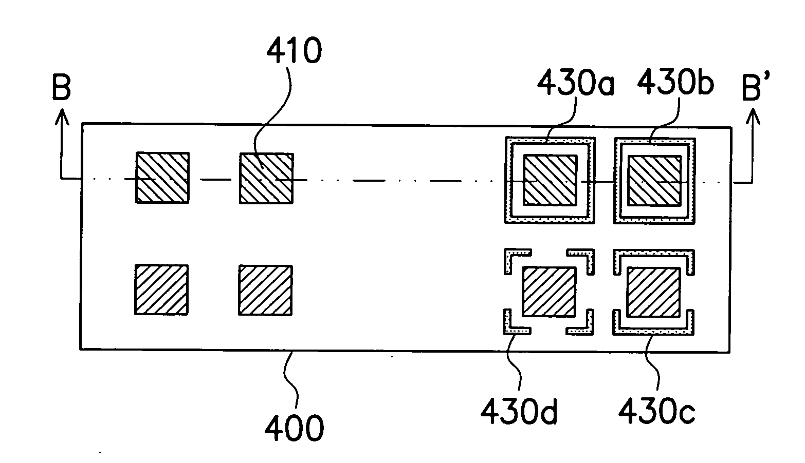
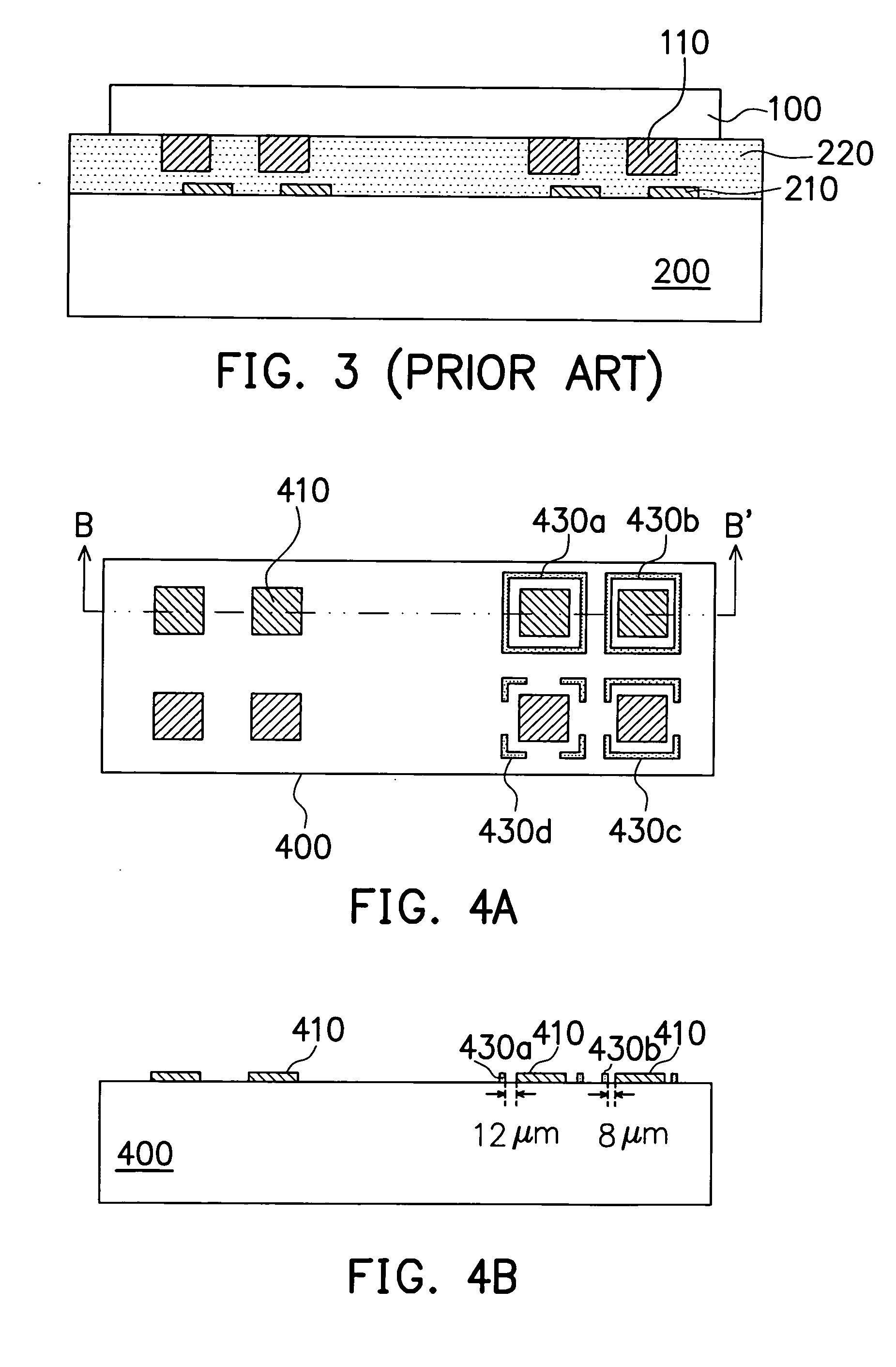
[0025]FIG. 5 is a schematic local cross-sectional view of a flat panel display (FPD) according to one embodiment of the present invention. FIG. 4A is a schematic local schematic top view of a flat display panel according to one embodiment of the present invention. It is noted that, the components, which are well known to those skilled in the art are omitted in these drawings. FIG. 4B is a schematic cross-sectional view along line B-B′ of FIG. 4A. Referring to FIG....


PUM


Abstract

A method of correcting bonding misalignment between flat display panel and driver IC is provided. First, the contact pads of the bonding flat display panel and the bumps of the driver IC are bonded, wherein the flat display panel further includes a plurality of alignment marks around each contact pad. A bonding misalignment variation between the flat display panel and the driver IC may be identified by matching the position of the alignment mark and the position of the corresponding bump. Thereafter, a correction may be performed according to the bonding misalignment variation.

Description

BACKGROUND OF THE INVENTION [0001] 1. Field of the Invention [0002] The present invention relates to a method of correcting bonding misalignment of a flat panel display (FPD). More particularly, the present invention relates to a method of correcting bonding misalignment between a flat panel display (FPD) or a flat display panel and a driver IC. [0003] 2. Description of Related Art [0004] Conventionally, liquid crystal display (LCD) panel has been broadly applied for a variety of consumer electronics or computer products since the LCD panel has the advantages of light weight, thin thickness, small size, low driving voltage, low power consumption and broad application, especially for the notebook or portable computer. [0005] In recent years, the chip on glass (COG) method has been developed for the bonding of the driver ICs to the display panel. Therefore, the thickness of the LCD panel is reduced and the reliability thereof is increased. The chip on glass (COG) method is performed b...

Claims


Application Information

Patent Timeline
Patent Type & Authority Applications(United States)
IPC IPC(8): H01J1/62H01J63/04
CPCH05K13/0486G02F1/13452
Inventor WEN, YU-LIANGTU, CHIN-CHUNGHUANG, ZHENG-JIEWANG, HUANG-CHANG
Owner CHUNGHWA PICTURE TUBES LTD
Why Eureka
Try Eureka