Area array routing masks for improved escape of devices on PCB

a technology of area arrays and masks, applied in the field of area array routing masks for improved, can solve problems such as and achieve the effect of reducing the number of pcb layers

Inactive Publication Date: 2007-03-15
ALCATEL LUCENT SAS
View PDF4 Cites 9 Cited by
  • Summary
  • Abstract
  • Description
  • Claims
  • Application Information

AI Technical Summary

Benefits of technology

[0013] Preparing a package of BGA pin-out maps which anticipate the effect of existing fixed pins and derives the resulting optimum pin location assignment. The package of pin-out maps, in which each pin-out map includes an indication of the best routing for circuits from a given component to be mounted to a PCB.
[0014] The said package of pin-out maps are also applied during the area array pin assignment phase, thereby making the area array package capable of supporting the optimum routing configuration proposed by the pin-out maps.
[0015] Applying said package of pin-out maps during a PCB design phase so that the optimum circuit routing to each pin is achieved, thereby completing the strategy layed out by the proposed pin-out maps, resulting in a lower number of PCB layers.

Problems solved by technology

However, since little or no guidance to this effect is provided at the pin-out determination stage, each device pin-out is usually sub-optimal in terms of ease of routing the PCB.
However, where multiple pin-out options exists that are equivalent under these criteria, there exists an opportunity to consider PCB routing issues, and possibly reduce the PCB layer count provided that some guidance is given to this end.

Method used


Image

  • Area array routing masks for improved escape of devices on PCB
  • Area array routing masks for improved escape of devices on PCB
  • Area array routing masks for improved escape of devices on PCB

Examples


Embodiment Construction

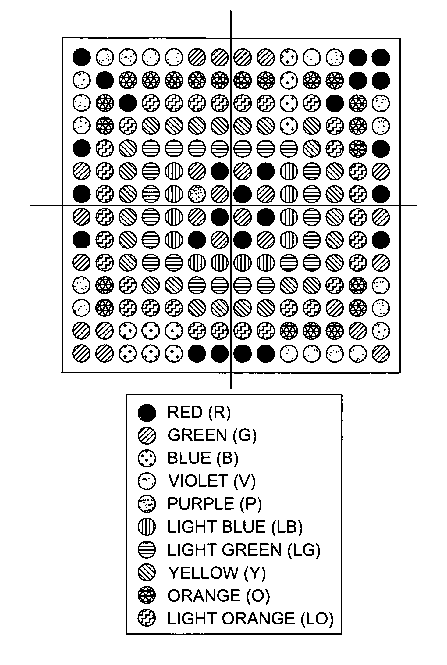
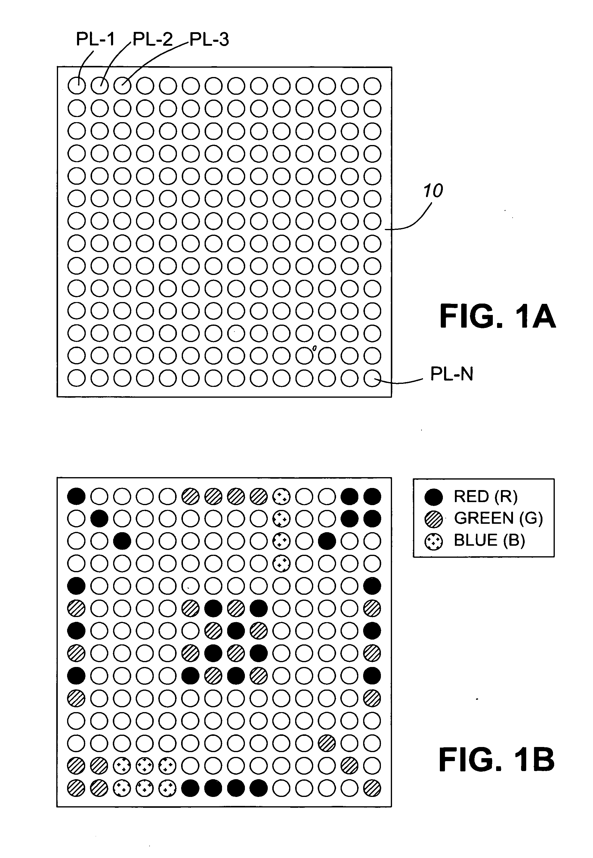
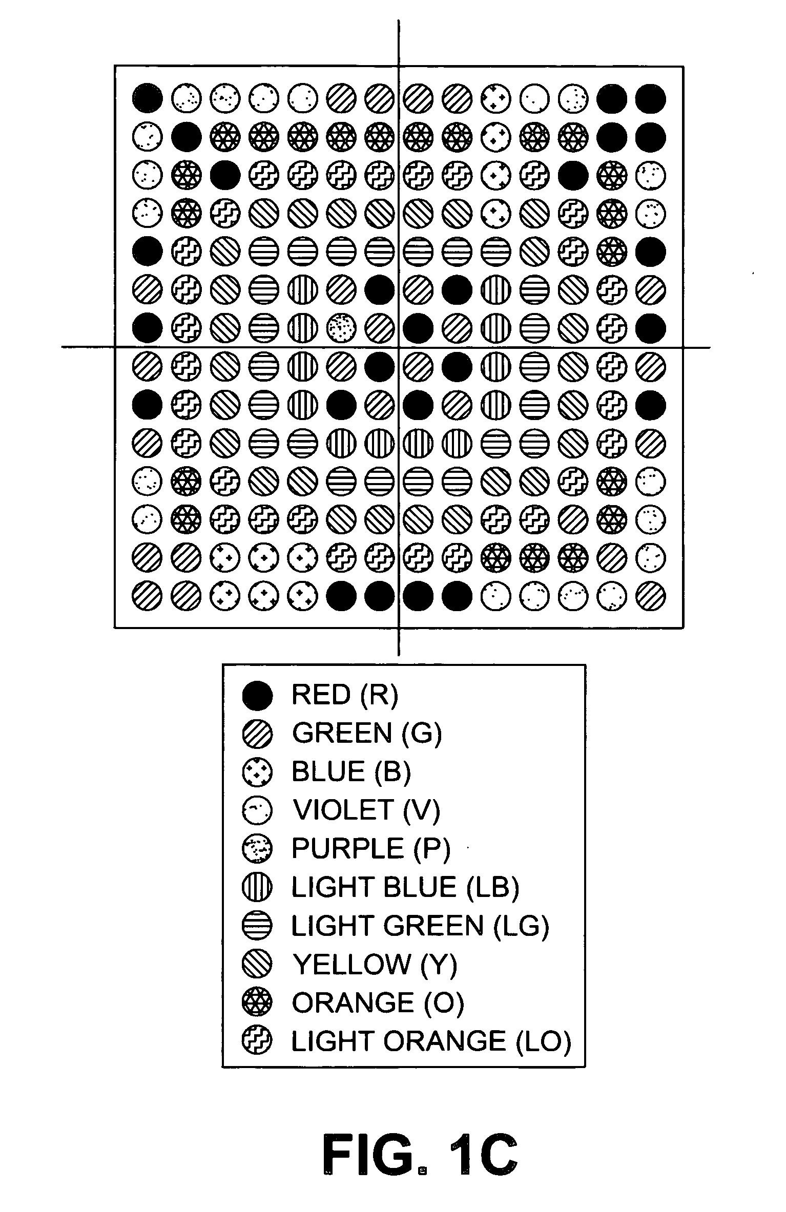
[0032] The invention provides package pin-out maps and a method of determining them. Each of the maps shows areas of equal routing ease for a given package type. Like areas are coded with the same color for manual pin-out determination, whereas they would have like numeral priority for an automated procedure. When determining the pin-out of a device, the areas of easiest routability are used first, and then areas of successively less routability as needed until all pin placements have been assigned. Some locations are predefined, such as power and ground pins, as well as high speed buses, clocks, etc. Areas of easiest routability are generally at the periphery of the package and ease of routability lessens towards inward layers barring any obstacles such as the aforementioned predefined locations. Maps can also be provided for no-connect (NC) pins to create channels for routing signal traces.

[0033] As an example, a study was done on a typical PCB. With a worst case pin-out the PCB ...


PUM


Abstract

A method for optimizing area array device pin utilization and reducing the number of layers on a multilayered PCB comprising: preparing a package of BGA pin-out maps which anticipate the effect of existing fixed pins and derives the resulting optimum pin location assignment. Each pin-out map includes an indication of the best routing for circuits from a given component to be mounted to a PCB. Applying the package of pin-out maps during an area array pin assignment phase, thereby making an area array package capable of supporting the optimum routing configuration proposed by the pin-out maps. Applying the package of pin-out maps during a PCB design phase so that the optimum circuit routing to each pin is achieved, thereby completing the strategy layed out by the proposed pin-out maps, resulting in a lower number of PCB layers.

Description

REFERENCE TO RELATED PATENT APPLICATIONS [0001] The present application is related to the following U.S. patent applications which are assigned to the assignee hereof: [0002] U.S. patant application Ser. No. 10 / 991,360 filed Nov. 19, 2004, inventor Paul Brown, entitled OFF-WIDTH PITCH FOR IMPROVED CIRCUIT CARD ROUTING; [0003] U.S. patant application Ser. No. 11 / 041,727 filed Jan. 25, 2005, inventor Alex Chan, entitled OFF-GRID DECOUPLING OF BALL GRID ARRAY (BGA) DEVICES; [0004] U.S. patent application Ser. No. 11 / 200,041 filed Aug. 10, 2005, inventor Paul Brown, entitled USING ROWS / COLUMNS OF MICRO-VIAS TO CREATE PCB ROUTING CHANNELS IN BGA INTERCONNECT GRID (Micro-Via Channels); and [0005] U.S. patent application Ser. No. 11 / 200,044 filed Aug. 10, 2005, inventor Paul Brown, entitled ALTERNATING MICRO-VIAS AND THROUGHBOARD VIAS TO CREATE PCB ROUTING CHANNELS IN BGA INTERCONNECT GRID.BACKGROUND AND BRIEF DESCRIPTION OF THE INVENTION [0006] High pin count devices, typically in excess ...

Claims


Application Information

Patent Timeline
Patent Type & Authority Applications(United States)
IPC IPC(8): H01L23/48
CPCG06F17/5068H01L23/49822H01L23/49838H05K1/112H05K3/0005H01L2924/0002H05K2201/09227H05K2201/10734H01L2924/00G06F30/39
Inventor BROWN, PAUL JAMES
Owner ALCATEL LUCENT SAS
Why Eureka
Try Eureka