Semiconductor device having metallic plate with groove

Active Publication Date: 2007-03-15
DENSO CORP
View PDF5 Cites 42 Cited by
  • Summary
  • Abstract
  • Description
  • Claims
  • Application Information

AI Technical Summary

Benefits of technology

[0014] In the above device, the solder member is prevented from expanding outside the semiconductor element. Thus, a

Problems solved by technology

Thus, short-circuit in the element may be occurred.
Further, in another semiconductor device having a semiconductor ele

Method used


Image

  • Semiconductor device having metallic plate with groove
  • Semiconductor device having metallic plate with groove
  • Semiconductor device having metallic plate with groove

Examples


Embodiment Construction

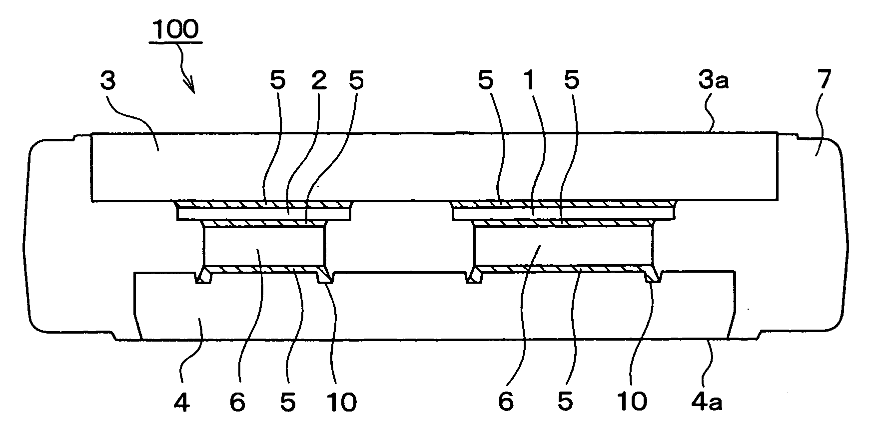
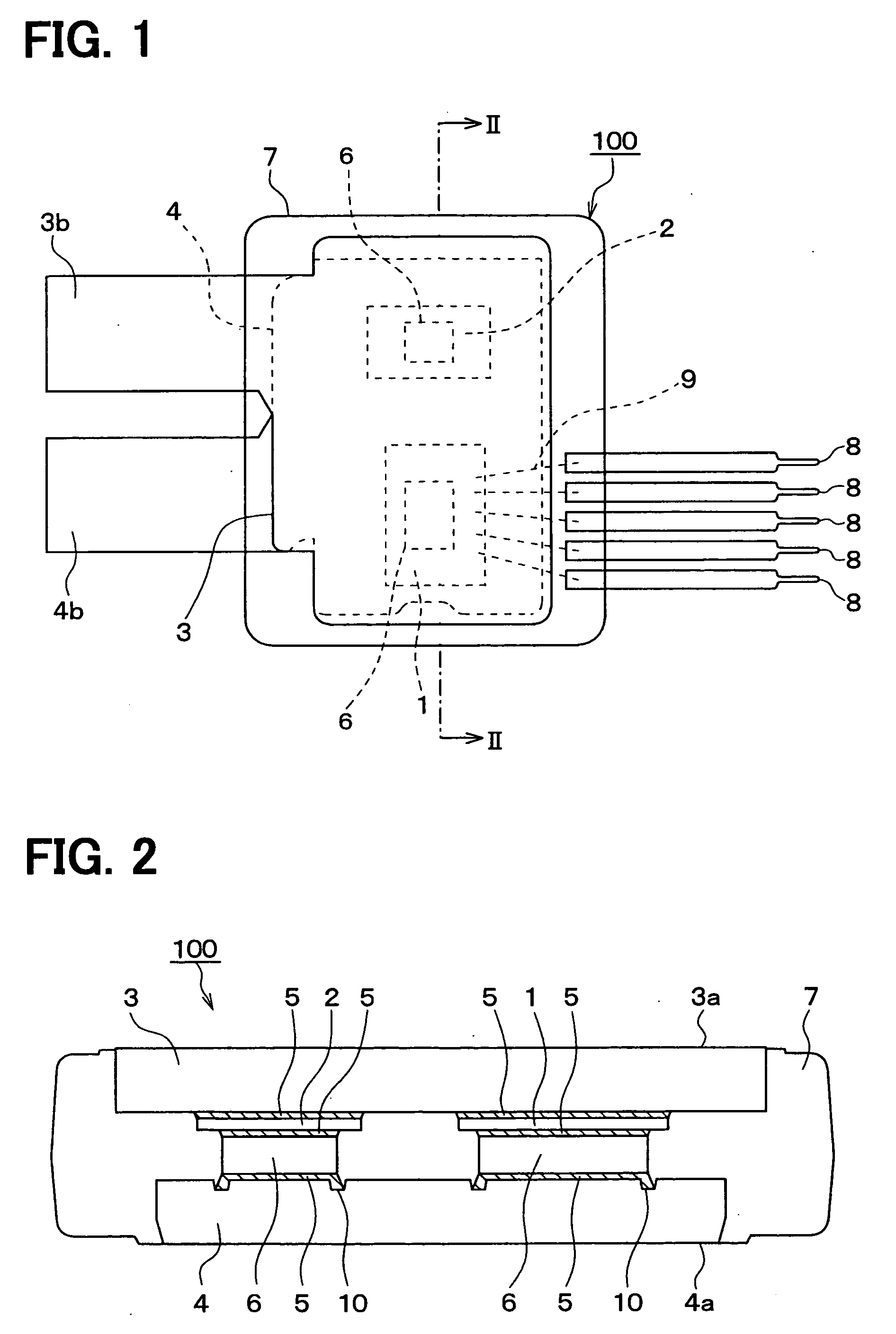
[0031] A semiconductor device 100 according to a first example embodiment is shown in FIGS. 1 to 4. In FIG. 1, each element in the device 100 is drawn through a resin mold 7. FIG. 4 shows a block 6 on a first semiconductor side. This device 100 is suitably used for an in-vehicle device mounted on an automotive vehicle so that the device 100 controls and drives electronic equipment in the vehicle.

[0032] The device 100 includes first and second semiconductor elements 1, 2, which are arranged on a certain plane of the device 100. In this embodiment, the first semiconductor element 1 is an IGBT (i.e., insulated gate bipolar transistor), and the second semiconductor element 2 is a FWD (i.e., free wheeling diode).

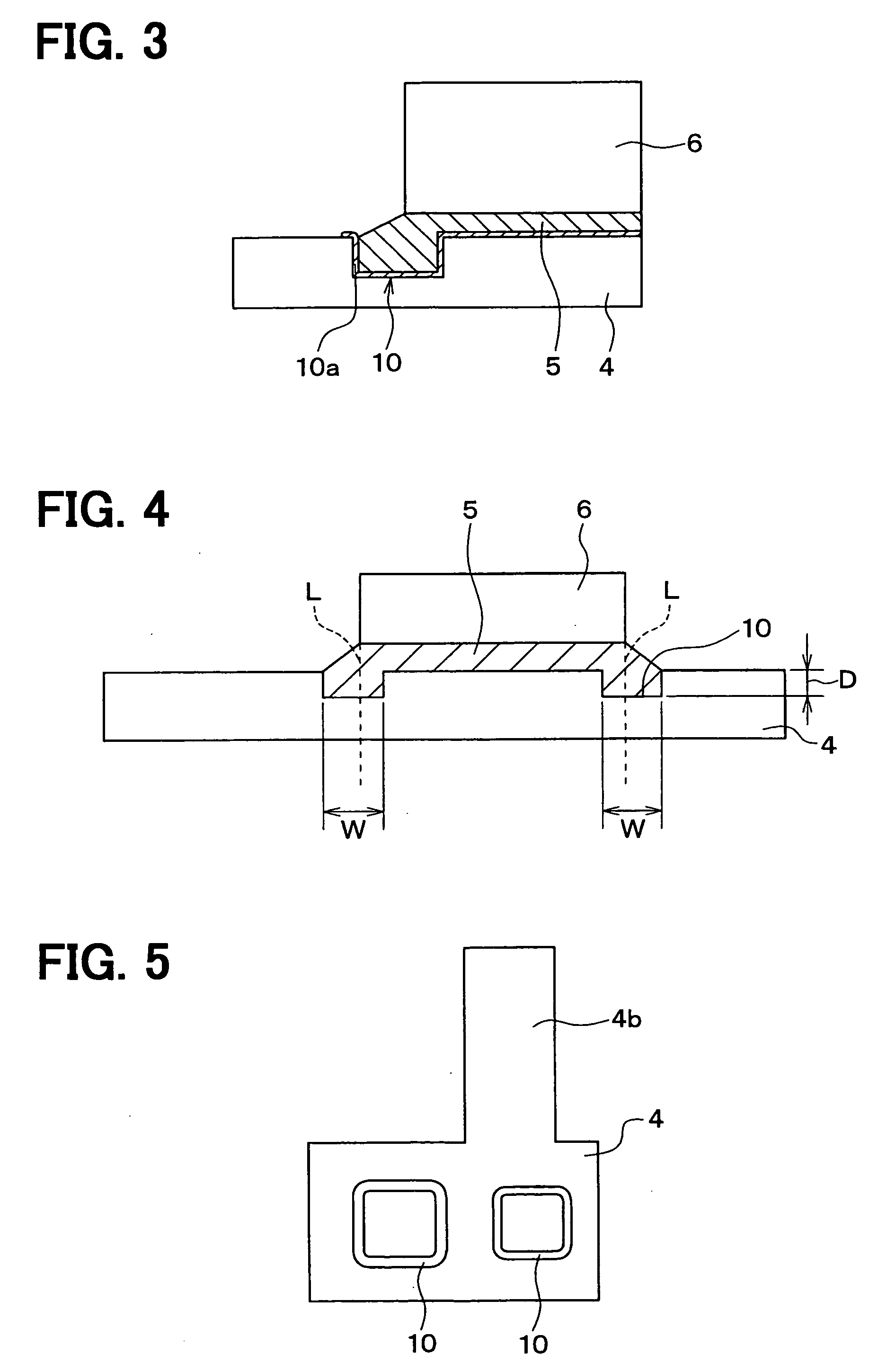
[0033] Both sides of each semiconductor element 1, 2 are covered with electrodes of the element 1, 2 and a pair of metallic plates 3, 4. Thus, both sides of the element 1, 2 are sandwiched between the metallic plates 3, 4. The metallic plates 3, 4 are made of conventional mater...


PUM


Abstract

A semiconductor device includes: first and second metallic plates, each of which includes a heat radiation surface and an inner surface; a semiconductor element between the metallic plates; a block between the second metallic plate and the semiconductor element; a solder member between the second metallic plate and the block; and a resin mold. The heat radiation surface is exposed from the resin mold. The second metallic plate includes a groove for preventing the solder member from expanding outside of the block. The groove is disposed on the inner surface and disposed on an outer periphery of the block. The second metallic plate further includes an inner surface member on an inner surface of the groove. The inner surface member has a solder wettability, which is larger than a solder wettability of the block.

Description

CROSS REFERENCE TO RELATED APPLICATIONS [0001] This application is based on Japanese Patent Applications No. 2005-263635 filed on Sep. 12, 2005, and No. 2006-175050 filed on Jun. 26, 2006, the disclosures of which are incorporated herein by reference. FIELD OF THE INVENTION [0002] The present invention relates to a semiconductor device having a metallic plate with a groove. BACKGROUND OF THE INVENTION [0003] A semiconductor device includes a metallic plate and a semiconductor element. The semiconductor element is bonded to the metallic plate with a solder so that a heat generated in the semiconductor element is radiated from the metallic plate. The device is disclosed in JP-2005-123233. The device further includes another metallic plate so that the semiconductor element is sandwiched between a pair of the metallic plates. A block is inserted between one of the metallic plates and the semiconductor element. The one of the metallic plates is bonded to the block with a solder. A pair o...

Claims


Application Information

Patent Timeline
IPC IPC(8): H01L23/52
CPCH01L23/051H01L23/492H01L23/49541H01L24/32H01L24/33H01L24/83H01L2224/27013H01L2224/29111H01L2224/32014H01L2224/32057H01L2224/48091H01L2224/48247H01L2224/49171H01L2224/73265H01L2224/83051H01L2224/83385H01L2224/83801H01L2924/01005H01L2924/01029H01L2924/01042H01L2924/01047H01L2924/0105H01L2924/01074H01L2924/01078H01L2924/01079H01L2924/01082H01L2924/13055H01L24/48H01L2224/2919H01L2224/32245H01L2924/01006H01L2924/01019H01L2924/01023H01L2924/01033H01L2924/014H01L2924/0665H01L24/49H01L2224/83455H01L2924/15747H01L2224/26175H01L2224/291H01L2924/1305H01L23/49503H01L23/49513H01L23/49562H01L23/49575H01L2224/33181H01L2224/92147H01L2924/00014H01L2924/00H01L2924/0132H01L2224/83H01L2924/181H01L2224/2612H01L2924/00012H01L2224/45099H01L2224/45015H01L2924/207
Inventor OKUMURA, TOMOMISAKAMOTO, YOSHITSUGUHIRANO, NAOHIKOMAMITSU, KUNIAKI
Owner DENSO CORP
Why Eureka
Try Eureka