Electronically addressable microencapsulated ink and display thereof

a technology of microencapsulated ink and electronic address, which is applied in the field of circuit board manufacturing, can solve the problems of inability to lay logic elements onto an arbitrary surface, no direct electronically addressable contrast medium, and inability to manufacture etched devices on arbitrary surfaces, etc., and achieve the effect of inexpensive display

Inactive Publication Date: 2007-03-15
E INK CORPORATION
View PDF99 Cites 111 Cited by
  • Summary
  • Abstract
  • Description
  • Claims
  • Application Information

AI Technical Summary

Benefits of technology

[0008] In one embodiment this invention provides for a microencapsulated electric field actuated contrast ink system suitable for addressing by means of top and bottom electrodes or solely bottom electrodes and which operates by means of a bichromal dipolar microsphere, electrophoretic, dye system, liquid crystal, electroluminescent dye system or dielectrophoretic effect. Such an ink system may be useful in fabricating an electronically addressable display on any of a large class of substrate materials which may be thin, flexible and may result in an inexpensive display.

Problems solved by technology

Such a technology is not amenable to laying down logic elements onto an arbitrary surface due to the presence of the vacuum requirement and the etch step.
No such directly electronically addressable contrast medium however is amenable to printing onto an arbitrary surface.
In the first case, such etched devices suffer from their inability to be fabricated on arbitrary surfaces.
In the second case, non-etched devices suffer from the inability to incorporate drive logic and electronic control directly onto the actuating surface.

Method used


Image

  • Electronically addressable microencapsulated ink and display thereof
  • Electronically addressable microencapsulated ink and display thereof
  • Electronically addressable microencapsulated ink and display thereof

Examples


Embodiment Construction

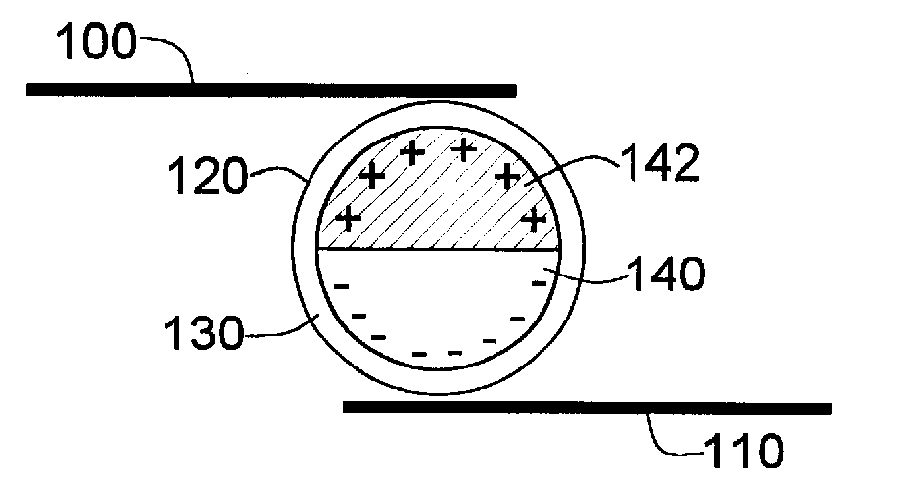
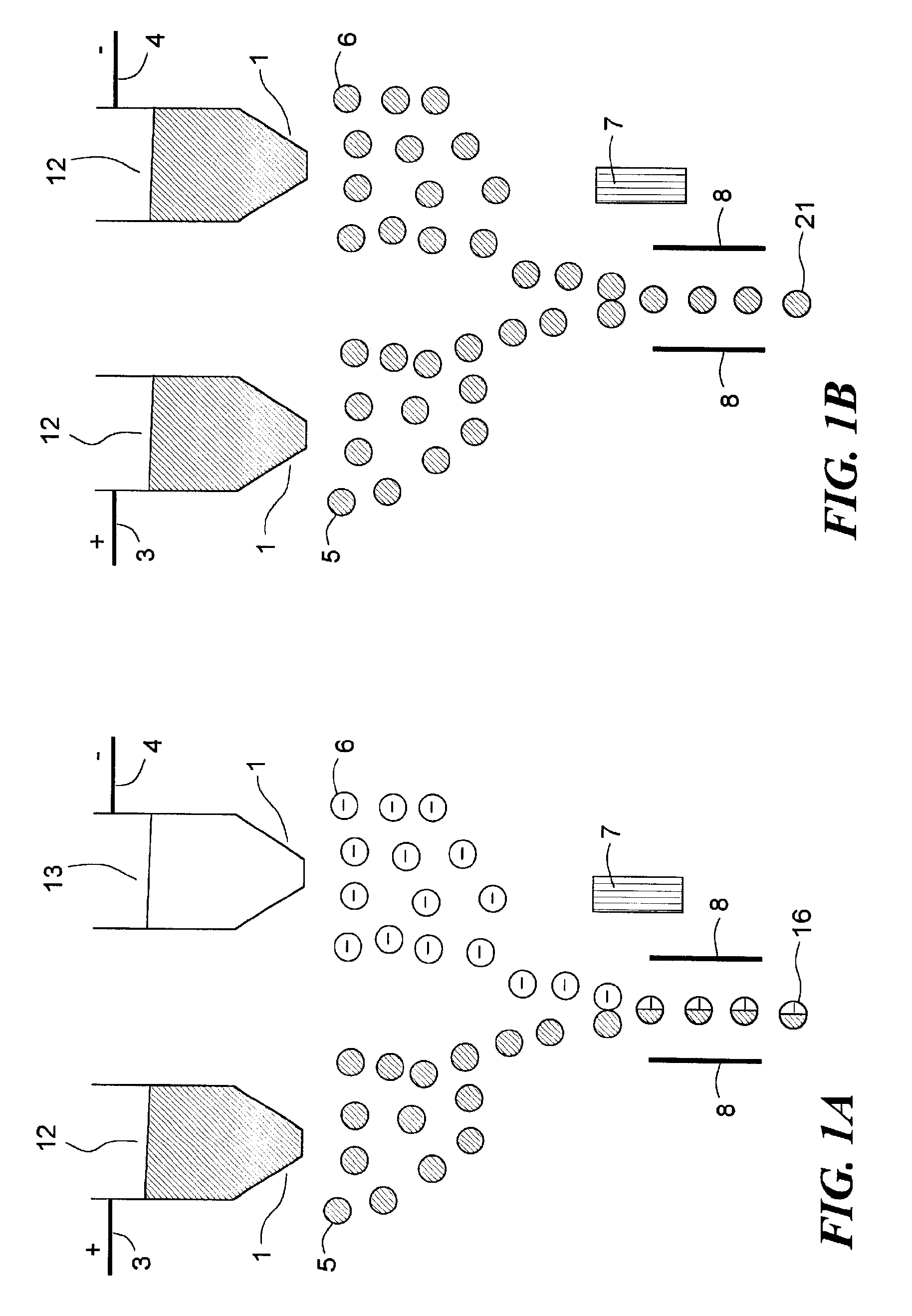
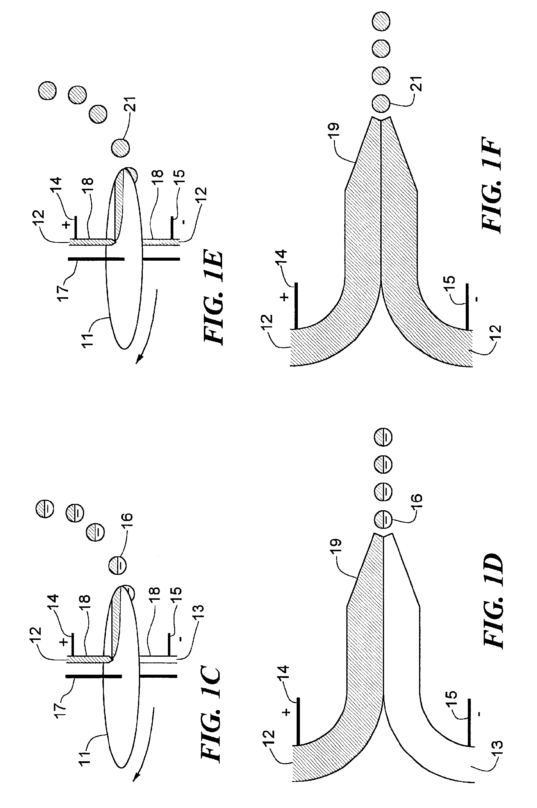
[0036] Means are known in the prior art for producing bichromal particles or microspheres for use in electronic displays. Such techniques produce a particle that does not have an implanted dipole moment but rather relies in general on the Zeta potential of the material to create a permanent dipole. Such a scheme suffers from the fact that it links the material properties to the electronic properties thus limiting the size of the dipole moment which may be created. FIG. 1 details means of producing particles, either bichromal as might be used in an electrostatic display, or monochromal as might be used in a dielectrophoretic display, with an implanted dipole moment.

[0037] Referring to FIG. 1A, atomizing nozzles 1 are loaded with materials 12 and 13 which may be differently colored. A first atomizing nozzle may be held at a positive potential 3 and a second nozzle may be held at a negative potential 4. Such potentials aid in atomization and impart a charge to droplets which form from...


PUM

PropertyMeasurementUnit
dielectric constantaaaaaaaaaa

Abstract

A system of electronically active inks is described which may include electronically addressable contrast media, conductors, insulators, resistors, semiconductive materials, magnetic materials, spin materials, piezoelectric materials, optoelectronic, thermoelectric or radio frequency materials. We further describe a printing system capable of laying down said materials in a definite pattern. Such a system may be used for instance to: print a flat panel display complete with onboard drive logic; print a working logic circuit onto any of a large class of substrates; print an electrostatic or piezoelectric motor with onboard logic and feedback or print a working radio transmitter or receiver.

Description

REFERENCE TO RELATED APPLICATIONS [0001] This application is a continuation of copending application Ser. No. 10 / 652,218, filed Aug. 29, 2003, which is a continuation of U.S. Ser. No. 10 / 200,571, filed Jul. 22, 2002 (now U.S. Pat. No. 6,652,075), which is a continuation of U.S. Ser. No. 09 / 471,604, filed Dec. 23, 1999 (now U.S. Pat. No. 6,422,687), which is a divisional of U.S. Ser. No. 08 / 935,800, filed Sep. 23, 1997 (now U.S. Pat. No. 6,120,588), which claims priority to U.S. Provisional Application No. 60 / 035,622, filed Sep. 24, 1996, and claims priority to and is a continuation-in-part of International Application PCT / US96 / 13469, filed Aug. 20, 1996, which claims priority to U.S. Provisional Application No. 60 / 022,222, filed Jul. 19, 1996, the entire disclosures of which applications are incorporated herein by reference in their entirety.BACKGROUND OF INVENTION [0002] Currently, printing of conductors and resistors is well known in the art of circuit board manufacture. In order ...

Claims


Application Information

Patent Timeline
Patent Type & Authority Applications(United States)
IPC IPC(8): G09G3/34B41J2/01B41J2/02B41J3/407B41M5/00C09D11/00G02B26/02G02F1/13G02F1/1334G02F1/1343G02F1/167G02F1/16757G02F1/1679G04B47/00G04G9/00G09F9/37H01L51/05H05K1/09H05K3/10H05K3/12
CPCB41J2/01H05K3/1241B41J3/4076B82Y20/00C09D11/30C09D11/50G02B26/026G02F1/1334G02F1/13439G02F1/167G02F1/19G04B47/00G09F9/372G09G3/344G09G2380/04H01L51/0508H05K1/097H05K3/105B41J2/02G02F1/1679G02F1/16757H10K10/46
Inventor JACOBSON, JOSEPH M.
Owner E INK CORPORATION
Why Eureka
Try Eureka