Method for manufacturing FFS mode LCD

a manufacturing method and ffs mode technology, applied in the field of lcd manufacturing, can solve the problems of image sticking, unbalanced driving voltage, and how to develop a manufacturing method for ffs mode lcd with less dielectric layers, and achieve the effect of reducing the number of dielectric layers and reducing image sticking

Active Publication Date: 2007-03-15
HANNSTAR DISPLAY CORPORATION
View PDF4 Cites 14 Cited by
  • Summary
  • Abstract
  • Description
  • Claims
  • Application Information

AI Technical Summary

Benefits of technology

[0007] In accordance with one aspect of the present invention, a method for manufacturing the FFS mode LCD is provided. The provided method is able to reduce the number of dielectric layers between the common electrode and the pixel electrode on the LCD, and thus the image sticking is reduced accordingly.

Problems solved by technology

The driving voltage becomes unbalanced between the odd (positive) frame and the even (negative) frame due to the thick dielectric layers, which in turn give rise to the image sticking.
From the above description, it is known that how to develop a method for manufacturing the FFS mode LCD with less dielectric layers has become a major problem to be solved.

Method used


Image

  • Method for manufacturing FFS mode LCD
  • Method for manufacturing FFS mode LCD
  • Method for manufacturing FFS mode LCD

Examples


embodiment i

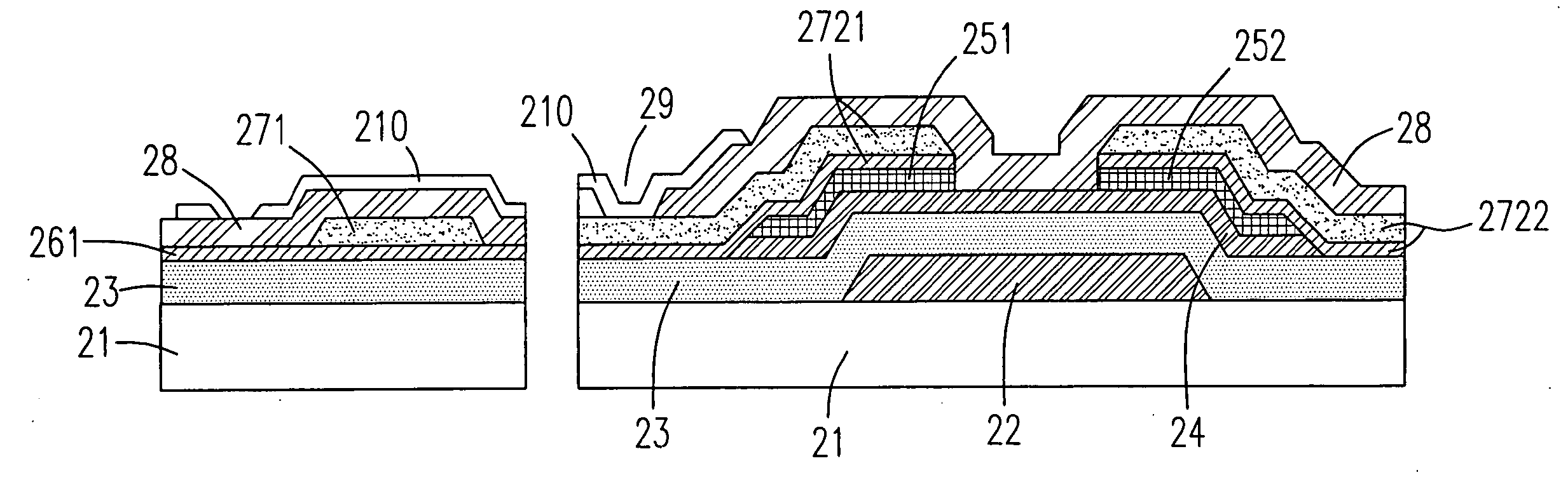
[0042] Please refer to FIG. 2(a), which shows a top view of the array structure of the FFS mode LCD according to a first preferred embodiment of the present invention. The FFS mode LCD has a plurality of pixels, wherein each pixel is surrounded by a plurality of gate lines 22 and a plurality of data lines 272, and includes a common electrode 26, a pixel electrode 210 with a plurality of openings, a common line 271 parallel to the data lines 272 and a contact hole 29.

[0043] Please refer to FIG. 2(b), which shows a cross-sectional view along A-A line of FIG. 2(a). As shown in FIG. 2(b), the manufacturing steps of the FFS mode LCD are as follows. Firstly, a substrate 21 is provided and a first metal layer is applied thereon. Subsequently, the first metal layer is etched to form a plurality of gate lines 22, and then a gate insulating layer 23 is applied which covers the gate lines 22 and a part of the substrate 21. Next, a channel portion 24 and a doped portion 25 are sequentially for...

embodiment ii

[0045] Please refer to FIGS. 3(a)-3(e), which show the processes for defining the common electrode and the data lines simultaneously through the half-tone technology according to a second preferred embodiment of the present invention. As shown in FIG. 3(a), firstly, a semiconductor layer and a doped layer are sequentially formed on the gate insulating layer 23 and the substrate 21. Then, the semiconductor layer and the doped layer are sequentially etched to form a channel portion 24 and a doped portion 253 on one of the gate lines 22. Next, a first ITO layer 261 is formed on the doped portion 253 and the gate insulating layer 23, and then a second metal layer 2711 is formed on the first ITO layer 261. After that, a photo resistance layer 31 is formed on the second metal layer 2711, and then a first pre-determined position of the photo resistance layer 31 is totally etched and a second pre-determined position of the photo resistance layer 31 is partially etched via the half-tone tech...

embodiment iii

[0050] Please refer to FIG. 4(a), which shows a top view of the array structure of the FFS mode LCD according to a third preferred embodiment of the present invention. The FFS mode LCD includes a common electrode 47, a pixel electrode 410, a plurality of gate lines 42, a common line 461, a plurality of data lines 462 and a contact hole 49. Please refer to FIG. 4(b), which shows a cross-sectional view along A-A line of FIG. 4(a). As shown in FIG. 4(b), the manufacturing steps of the FFS mode LCD are as follows. Firstly, a substrate 41 is provided, and then the gate lines 42 and a gate insulating layer 43 are sequentially formed on the substrate 41. Next, a channel portion 44 and a doped portion 45 are sequentially formed on the gate insulating layer 43, wherein the doped portion 45 includes a first doped portion 451 and a second doped portion 452. After that, the data lines 462 and the common line 461 are simultaneously formed on the gate insulating layer 43, wherein the data lines 4...


PUM

PropertyMeasurementUnit
areaaaaaaaaaaa
transparentaaaaaaaaaa
insulatingaaaaaaaaaa

Abstract

In the present invention, a method for manufacturing a liquid crystal display is provided. The method includes steps of providing a substrate, forming a first metal layer on the substrate, etching the first metal layer to form a plurality of gate lines on the substrate, forming a common electrode on the substrate, forming a second metal layer on the substrate, etching the second metal layer to form a first electrode, a second electrode, a common line and a plurality of data lines on the substrate, and forming a pixel electrode overlapping the common electrode, wherein the gate lines intersect the data lines to form at least one enclosed area, the common electrode and the pixel electrode are positioned in the enclosed area, the first electrode is connected to the pixel electrode and the second electrode is connected to the data lines.

Description

FIELD OF THE INVENTION [0001] The present invention relates to a method for manufacturing the LCD, and more particularly to a method for manufacturing the FFS mode LCD. BACKGROUND OF THE INVENTION [0002] In the current display industry, the liquid crystal display (LCD) has gradually replaced the cathode ray tube (CRT) to become a mainstream product due to its excellent properties of low radiation and low power consumption. In the array structure of LCD, the FFS (Fringe Field Switching) mode is a promising structure owing to its high transmittance, wide viewing angle and low color shift. [0003] Please refer to FIG. 1(a), which shows a top view of the array structure of the FFS mode LCD in the prior art. The FFS mode LCD includes a common electrode 12, a pixel electrode 110, a plurality of gate lines 13, a common line 111, a plurality of data lines 17 and a contact hole 19. [0004] Please refer to FIG. 1(b), which shows a cross-sectional view along A-A line of FIG. 1(a). As shown in FI...

Claims


Application Information

Patent Timeline
Patent Type & Authority Applications(United States)
IPC IPC(8): H01L21/00
CPCG02F1/134363G02F1/1362G02F2001/134372G02F2001/133397G02F1/136227G02F1/133397G02F1/134372
Inventor SHIH, PO-SHENG
Owner HANNSTAR DISPLAY CORPORATION
Why Eureka
Try Eureka